


As useful and versatile as instrumentation amplifiers (IAs) are when it comes to interfacing to a transducer, there are constraints that hamper the design of variable gain IAs or programmable gain instrumentation amplifiers (PGIAs), also referred to as software programmable gain amplifiers (SPGAs) in some literature.
The need for such PGIAs arises because of the often-encountered case of adapting the circuit to a wide range of sensors or environmental conditions. With a fixed gain, the system designer may have to contend with suboptimal SNR, which could compromise precision.
Many of the techniques that are useful in creating an accurate and stable PGIA are discussed in another article from ADI, ‘Programmable Gain Instrumentation Amplifiers: Finding One that Works for You,’ which points out the possible pitfalls of such a design and presents a comprehensive survey of available solutions and techniques. In this article, we will present another tool and methodology to facilitate such work and go through the design steps that allow one to quickly home-in on the external component values needed to create a precise PGIA using a newly released instrumentation amplifier.
A new instrumentation amplifier architecture
One common instrumentation amplifier architecture is shown in Figure 1.
The gain is set by the value of the external resistor RG. To create a PGIA with such a device, one merely needs to switch the value of RG. This is commonly done using an analogue switch or a mux. However, some of the non-ideal behaviours of an analogue switch complicate this task – examples being the switch on-resistance, its channel capacitance, and the variation of channel resistance with applied voltage.
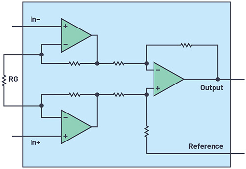
Above: Figure 1. Classic instrumentation amplifier
One variation on the standard instrumentation amplifier architecture is shown in Figure 2. Notice how the RG pins are broken up as ±RG,S and ±RG,F and individually pinned out and accessible from the outside of the device package.
A useful and important feature of the architecture shown in Figure 2 is the ability to configure the instrumentation amplifier so that it can switch between several distinct gain values while minimising any gain error because of the finite switch resistances. This feature can be used to create a PGIA.
As mentioned, any resistor programmable in-amp can be enabled to vary its gain by switching the value of the gain-setting resistor accordingly. However, there are significant drawbacks to this such as:
- Large gain error due to switch on-resistance (RON) nominal value and its variation.
- High gain values may be impossible to achieve due to the low switch RON values required.
- Signal distortion due to switch non-linearity. That is because signal current flows directly through RON and thus any variation in its value as a function of voltage causes distortion.
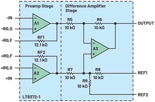
Above: Figure 2. LT6372-1 architecture allows access to some of the IA internal nodes
The LT6372-1 can alleviate these concerns when configured as a PGIA, shown in Figure 3, because of how the RG,F and RG,S pins are separately pinned out. In this schematic, the signal from a Wheatstone bridge, consisting of R5 to R8, is amplified with four possible gain values selectable by the user depending on which SW1 switch position is selected. The LT6372 family pinout allows one to create a PGIA that takes advantage of varying the ratio of RF/RG to get the desired gain values.
Furthermore, the U1, U2 analogue switch RON is minimised as a source of gain error because it can be placed in series with the input stage inverting terminal and its feedback resistor. Configured this way, RON is only a small fraction of the total internal 12.1kΩ feedback resistance and thus has little impact on gain error and drift. By the same token, distortion due to the switch non-linearity is minimised because of the RON value being a small fraction of the overall feedback resistance causing little or no effect due to variation of its value with voltage. Furthermore, the input stage of this device is comprised of a current feedback amplifier (CFA) architecture, which by its nature allows less variation in bandwidth or speed as gain is varied when compared to a traditional voltage feedback amplifier. All this culminates in the ability to create a precision PGIA with accurate gain steps using low cost external analogue switches.
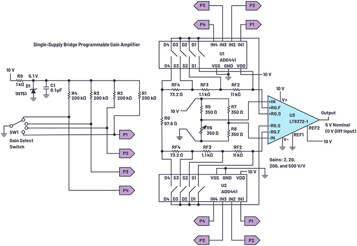
Above: Figure 3. LT6372-1 PGIA bridge interface with four gain settings
Figure 4 shows a simplified diagram of the PGIA to demonstrate how different taps of the resistor ladder, implemented by analogue switches (eight total) shorted two at a time to set the gain, configure the circuit. In this diagram, the two switch banks are depicted in one of the four possible gain values; that being with the –RG,S and +RG,S pins shorted to the RF3/RF4 junction.
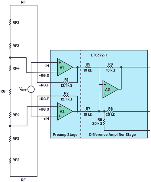
Above: Figure 4. LT6372-1 block diagram and simplified external connection (gain switches not shown) for the PGIA
Design steps to compute external resistors
Figure 3 shows the complete PGIA configuration, including the switches required, which can accommodate an arbitrarily large gain range. Four possible gain values are included here, but it is possible to increase that number by adding more switches to the design. As noted earlier, the feature of allowing access to the RG,F and RG,S pins enables one to increase RF for large gains, and to reduce RG for low gains to create a versatile PGIA. For purposes of gain computation, one can consider the feedback resistor to be the internal 12.1kΩ trimmed resistance plus other resistances in series with RG,F on its way to reach the RG,S terminal. Conversely, the gain setting resistor is the total resistance seen between +RG,S and –RG,S. This is summarised as:
- RF = 12.1kΩ + resistance between RG,F and RG,S on each of the two input amps.
- RG = resistance between +RG,S and –RG,S.
Gains from greater than 1V/V up to 1,000V/V are possible with this configuration. With the switches set to short pins S3, and D3 on both U1 and U2 switches, here are the corresponding RF and RG values and the resulting gain:
- RF = 12.1kΩ + 11kΩ + 1.1kΩ = 24.1kΩ
- RG = 73.2Ω + 97.6Ω + 73.2Ω = 244Ω
- G = 1+ 2RF/RG = 1 + 2 × 24.1kΩ/244 Ω = 199V/V.
It is easy to see that deciding on which values to use for the external resistors is an iterative and interdependent process where the possible gain values interact and influence the choice of resistors to use. Some common gain value component values are tabulated in Table 1 for easy reference, but a multitude of other gain combinations (G) are also possible.
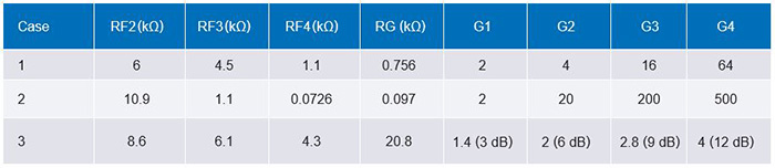
Above: Table 1. Component values for some PGIA gain combinations
Procedure for determining the value of the PGIA
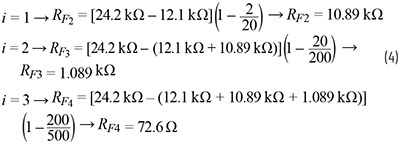
The individual resistors in the gain network can be calculated sequentially using the formula given in Equation 1. The equation determines the resistors as labelled in Figure 3, where Case 2 from Table 1 (gains 2, 20, 200, and 500V/V) is used as a worked-out example. The feedback resistors and the gain setting resistors are interactive; thus, the formula must be a series where the present term is dependent on the preceding term(s). The formula is given by:
![]()
Here are some definitions:
RF1 = 12.1kΩ (internal to the LT6372-1)
M: Number of gains (four in this case)
Gi: The gain instance (either 2, 20, 200, or 500 V/V for G1 – G4 respectively of this example)
i: Varies from 1 to (M-1) to compute RFi + 1
![]()
Equation 1 can be used to calculate the necessary feedback resistors for any set of gains. A dummy variable (j) serves as a counter to keep a running total of the preceding feedback resistors.
Before making any calculations, it is advised to draw a resistor network similar to the network in Figure 3. The network will have (2 × M) – 1 resistors, where M = number of gains. For this example, M = 4 and, therefore, the resistor string will have seven resistors. Equation 1 needs to be evaluated for i = 1 → (M – 1).
G1 = 2, G2 = 20, G3 = 200, G4 = 500V/V.
From Equation 2:
![]()
Evaluating Equation 1 iteratively from i = 1 → (M-1).
The centre resistor RG can then be computed using the following:
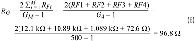
With this last computation, all four resistor values shown in Table 1 are computed and the design computation is finished.
Measured performance plots
Here are some plots showing the performance that can be achieved with this PGIA configuration:
With the switch capacitances of ADG444, at the lowest gain setting (G1 = 2V/V) the small signal frequency response shows some appreciable peaking (see Figure 7). This behaviour only shows with the lower gain settings where the LT6372-1 bandwidth extends high enough to be affected by the pF range capacitance of the switch. Choosing a lower capacitance switch (for example, ADG611/ ADG612/ADG613 with 5pF on capacitance) or alternatively limiting the lowest gain setting of the PGIA are ways to work around this side effect.
Conclusion
A method was introduced to add gain select ability to instrumentation amplifiers by utilising the pinout feature of a newly released set of devices, the LT6372 family. Characteristics of such a PGIA were analysed, and the design steps were spelled out along with performance measurements. The LT6372-1 is uniquely qualified for such a solution as it is highly linear and offers precise DC specifications and performance.
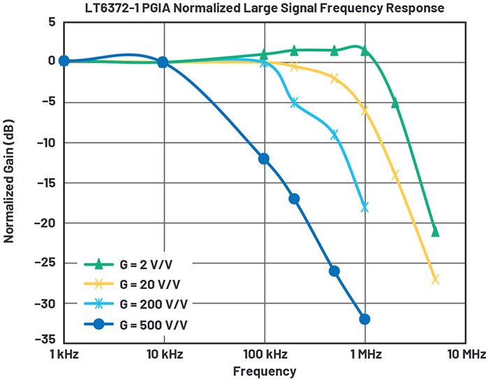
Above: Figure 5. PGIA large signal frequency response
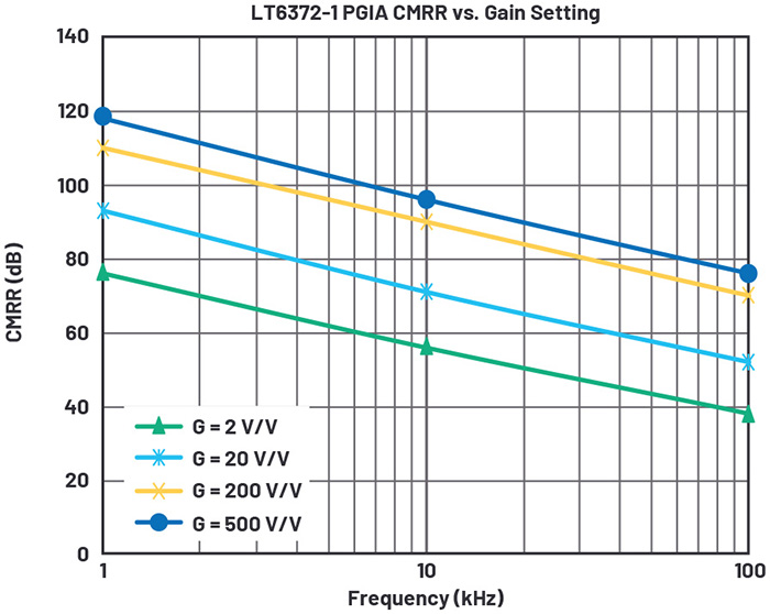
Above: Figure 6. PGIA CMRR vs. frequency
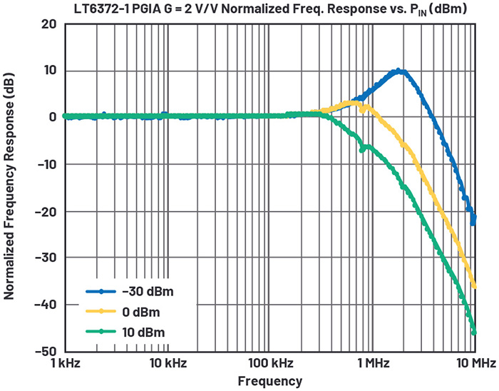
Above: Figure 7. PGIA small signal low gain peaking