


For example, a common IIoT edge application is processing of periodic analogue-to-digital converter (ADC) sensor data. For high-precision analogue data, the mathematical processing, interpretation, and interpolation of hundreds of ADC data points can significantly load the edge host processor, potentially impacting the performance of the whole network. In addition, high-accuracy ADCs can require self-calibration to be performed in the firmware of the IoT endpoint’s host microcontroller, which can delay all edge processing until the calibration is complete.
This article will show developers how to use precision analogue microcontrollers from Analog Devices as smart ADC peripherals. It will explain how the features of these analogue microcontrollers make them applicable for use as single-chip data acquisition systems, that easily interface to the IIoT endpoint microcontroller, and can perform edge processing functions such as ADC data point processing and self-calibration, with no performance impact on the main endpoint microcontroller.
Why process analogue sensor data at the edge?
As IIoT systems are becoming more complex, so too is the data they need to process. For industrial control applications, valves and some motors are moving from open-loop to closed-loop systems where precision analogue sensors must detect minute valve or motor positions. For process control applications, increased processing has led to faster production lines and finer control of temperature, pressure, and actuators in the system.
In process control, the speed of the line (the process) is mostly dependent upon two factors: the mechanical ability of the machines and systems on the floor, and the efficiency of the IIoT networks that control the sensors and actuators in the machines and systems. In some cases, small improvements in the process can lead to increased production, but these improvements can be hindered by bottlenecks in the IIoT network. These bottlenecks can be reduced by performing more processing at the edge.
Edge processing at the IIoT endpoint is especially beneficial for processing analogue signals. Processing analogue data can be simple during the early stages of the IIoT development, but scalability is an issue: later improvements can lead to increased complexity of calculations. Sending all the raw analogue data over the network increases network traffic and processing all that data at the network hub processor takes up valuable compute time. For this reason, processing the analogue data at the edge is a practical way to make the network more efficient.
Use smart ADCs to process analogue data at the edge
Edge processing of hundreds of samples of ADC data can easily overwhelm the main microcontroller in the IIoT endpoint. For complex analogue sensors it’s a smart design decision to have an external ADC that also has its own processing capabilities. This not only takes a significant load off the IIoT endpoint microcontroller, but also makes self-calibration of the ADC easier.
For high-performance capture and processing of ADC data, Analog Devices has a line of precision analogue microcontrollers. The ADuCM360BCPZ128-R7 precision analogue microcontroller uses an Arm Cortex-M3 to control two 24-bit sigma-delta ADCs (Figure 1). The ADCs are capable of capturing 4 kilo-samples per second (kSPS) of analogue sensor data. The ADuCM360 also has a 12-bit digital-to-analogue converter (DAC) for generating accurate voltages for self-calibration. The microcontroller can operate from 1.8 to 3.6V and contains an internal 32 kilohertz (kHz) oscillator and an internal 16 megahertz (MHz) oscillator, reducing component count in space constrained systems.
The ADuCM360 has 128 kilobytes (Kbytes) of flash memory and 8 Kbytes of SRAM. A significant advantage of the ADuCM360 is that the flash memory locations can be written to directly, similar to writing to SRAM. This allows the firmware developer to easily partition blocks of the flash memory as program memory and also as EEPROM. In a data acquisition system, this allows the EEPROM partitioned blocks to be used to store ADC calibration data.
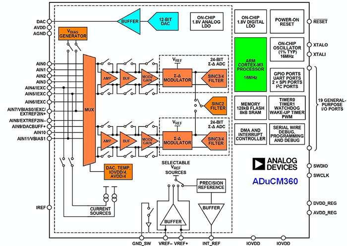
Above: Figure 1. The Analog Devices ADuCM360 is a complete low-power data acquisition system on a chip with an Arm Cortex-M3 core, two 24-bit sigma-delta 4 kSPS ADCs, and a 12-bit DAC. (Image source: Analog Devices)
The flash supports direct 32-bit erase and writes (16-bit and 8-bit erases and writes are not supported). The ability to write 32-bits at a time saves significant power in battery-powered applications, as flash write and erase operations draw a lot of current. This is a significant low-power advantage over flash microcontrollers that can only write and erase one block or page at a time.
The flash memory also supports conventional flash erase commands such as page erase, and mass erase of the entire flash memory array. With these capabilities, developers can easily write subroutines that can update the firmware based on commands sent over the serial port from the host microcontroller in the IIoT endpoint. This is important: if the ADuCM360 was unable to easily update its firmware through a serial port, it would severely limit its flexibility in a data acquisition system, as the capability to update the firmware controlling the ADC is just as important as the ADC itself.
An efficient single-chip data acquisition system
Both 24-bit ADCs are connected to an input multiplexer that supports a total of 11 single-channel or six differential inputs. There are four internal channels that can monitor the internal temperature sensor as well as monitor the output of the 12-bit DAC, and an internal low-drift bandgap reference. These can be used to perform a self-calibration of the ADCs. The DAC can be programmed to output a series of voltages which can be read by each of the ADCs. The ADCs can also sample the internal bandgap reference voltage. Firmware can process these readings so the ADCs can be calibrated over temperature, and the calibration constants stored in the EEPROM.
When used as a single-chip data acquisition system, the ADCs can be programmed to take continuous samples of analogue data as fast as 4 kSPS. An 11-channel direct memory access (DMA) controller can transfer that data to SRAM. Firmware can then apply the calibration constants stored in EEPROM to modify the data and correct for temperature if necessary. Firmware can then process the data as required by the application while the DMA transfers additional ADC data to SRAM.
Once data processing on the stored ADC data is complete, the result can either be sent to the serial interface to be transferred to the IIoT endpoint microcontroller, or if multiple data samples need to be transferred, the DMA can bulk transfer the data to the serial interface. In this manner, an efficient data acquisition system can sample and DMA transfer one set of ADC data to SRAM, process a second set of ADC data, and DMA transfer a third set of ADC data to the serial interface, all at the same time.
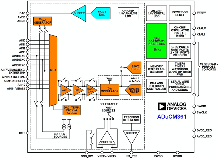
Above: Figure 2. The ADuCM361 is a complete data acquisition system on a chip, similar to the ADuCM360 except it has one 24-bit sigma delta ADC. This saves cost and power in applications that do not require the performance of two ADCs running simultaneously. (Image source: Analog Devices)
The analogue input signals can be amplified with a programmable gain amplifier (PGA) that can be set to powers of 2, supporting gain values of 2, 4, 8, 16, 32, 64, and 128. This allows the amplification of very small voltages for more accurate ADC sampling.
While additional features include a 16-bit six-channel pulse width modulation (PWM), 19 general purpose I/Os (GPIOs), two 16-bit general-purpose timers, a 32-bit wakeup/watchdog timer, and an external interrupt system, it’s important to keep the application firmware focused on supporting its main purpose of ADC capture and data processing. Tasking the ADuCM360 to perform additional functions not related to its main purpose of analogue data capture can easily lead to feature creep that interferes with that purpose, while also complicating firmware updates.
Ultra-low-power features and characteristics
Despite the high-end analogue features of the ADuCM360, it is still capable of low power consumption under high performance conditions. In normal operating mode, the Cortex-M3 core draws just 290 microamperes (µA)/MHz. With a system clock of 0.5MHz, both ADCs taking samples, all timers running, and a PGA gain of 4, when accessed from the SPI interface, the microcontroller draws only 1 milliamp (mA). This is with the input buffers off, as the buffer voltage storage adds to the power drain. When in hibernate mode with only the wake-up timer running, the microcontroller draws a mere 4µA. This makes the ADuCM361 appropriate for battery powered IIoT endpoints.
For less complex applications that do not require the speed of two ADCs, Analog Devices offers the ADUCM361BCPZ128-R7, which is the same as the ADuCM360 except it has only one sigma-delta 24-bit ADC (Figure 2).
In applications that do not require the high performance of having two 24-bit ADCs running at the same time, the ADuCM361 lowers system cost and board power consumption. The single ADC is also connected to an input multiplexer that supports a total of 11 single-channel or six differential inputs. It can also self-calibrate using the 12-bit DAC, internal bandgap reference, and temperature sensor.
The ADuCM361 is pin compatible with the ADuCM360. This allows a single PC board layout to be used for both products. This simplifies product development and bill of materials (BOM) as an IIoT endpoint manufacturer can use one PC board for two or more products.
Data acquisition system development
For product development, Analog Devices provides the EVAL-ADuCM360QSPZ evaluation kit. The evaluation board can interface to analogue sensors or external voltage sources for firmware development of the ADuCM360 and ADuCM361 analogue microcontrollers.
The evaluation kit is accessed by a host computer running Windows via a USB port. This allows the on-board ADuCM360 to be programmed with target firmware for testing and debugging. The EVAL-ADuCM360QSPZ has all pins of the ADuCM360 available on the PC board, including the serial I/O, so the eval board can be interfaced via I2C, SPI, or UART to a host microcontroller for real-time debugging. The host Windows computer can log the ADC data and can also debug the accuracy of the self-calibration routines.
Conclusion
Many IIoT endpoints used for high-end analogue applications such as process control need to do more edge processing on analogue sensor data captured using ADCs. The amount of ADC data and the complexity of the edge processing can overwhelm the IIoT endpoint main microcontroller. The main endpoint microcontroller can instead interface via a serial port to an analogue microcontroller that is a self-contained data acquisition system. This increases the performance of the endpoint and reduces network traffic, resulting in a more efficient IIoT network.