


Modern automotive and industrial systems require a stable voltage source even as the system input voltage sweeps from one extreme to another. In automotive systems, significant rail voltage variations can result from cold cranking startup, cylinder deactivation/activation in dynamic fuel management systems, or significant engine load changes. Similarly, in industrial applications, line brown-outs are a problem, and the switching on of motors in high power equipment can lead to serious drops of input voltage.
Even when power conversion systems cannot provide full power to the loads at low voltage inputs, many of these systems must remain operational, regardless of the input voltage level. For example, widely used high voltage boost and buck converters employ high voltage MOSFETs with a standard gate level. At input dropout, the bias voltage should stay above the 10V to keep the gate drivers operational. Critical digital control and information systems should be biased and functional regardless of the input conditions as well.
Circuit description
If the input voltage is not expected to fall below the desirable bias level and the goal of design is to have an external bias power supply to minimise the power dissipation of the switching controllers, then a straightforward buck converter can be employed.
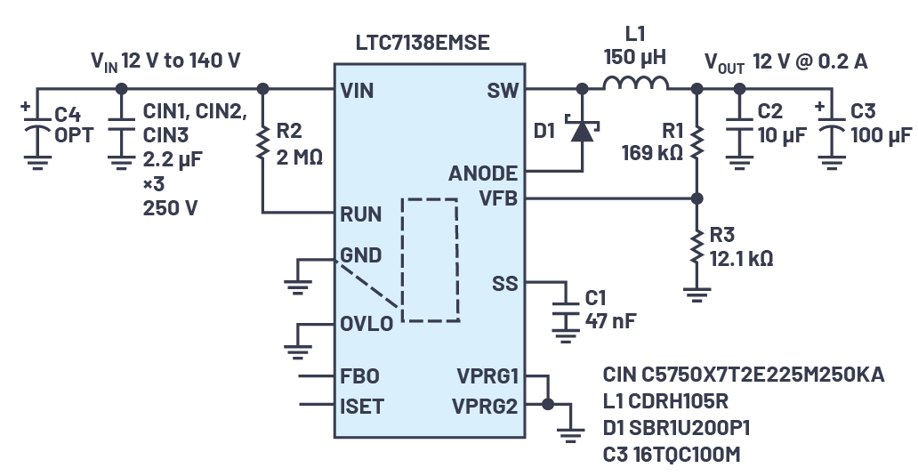 Figure 1: High voltage, buck-based bias circuit electrical schematic (V IN is 12.5V to 140V and the V OUT is 12V at 0.2A.
This approach is illustrated in Figure 1. The solution is centred around a high voltage buck-controller LTC7138 with internal switching transistors. The powertrain also includes inductor L1, diode D1, and output capacitors C2 and C3. To minimise the profile, to below 3mm, only ceramic capacitors were used in the input. An optional polarised capacitor can be used as well (for example, a cost-effective 22µF 200V, EMVE201 ARA220MKG5S), but it considerably increases the height of the bias power supply.
This circuit was verified and tested, with the waveforms illustrating the functionality of the circuit presented in Figure 2. The initial input voltage level of 100 V drops to 12 V, but the output provides 0.2 A of the stable 12 V voltage to the load.
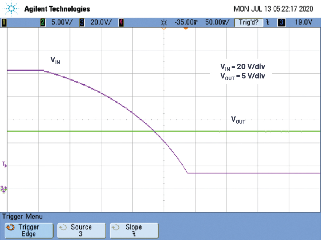
Figure 2: High voltage, buck-based bias circuit waveforms where the V IN is 20V/div, V OUT is 5V/div, and the time scale is 50ms/div.
The performance outlook of this design significantly changes if the input voltage drops below the desired bias level. In this case, using just the buck converter is not enough, because the output voltage follows the input when it falls below the desired output. Figure 3 illustrates a solution to this problem using a dual-stage bias power supply. The first, main stage is a high voltage step-down converter similar to what is shown in Figure 1. It is output connected to a boost converter and based on an LT8330 converter IC with integrated power transistor. The power train includes inductor L2, diode D2, and an output filter. The voltage stress on the components in the boost converter circuit is much lower compared to the buck front end, which permits selection of relatively inexpensive parts and reduces the overall cost.
The output of the buck converter in this circuit is set to 12.5V. However, the output of the boost converter is set to a lower voltage of 10.5V, enough for the load to function properly. The converters are never operational at the same time. If one is switching, the second is not.
In normal operating conditions (V IN > 12.5V), when the input voltage changes from 12.5 to 100V, only the buck converter is active, providing 12.5V to the load. The current flows to the load terminal V OUT through the inductor and diode of the boost converter. Due to relatively low current levels, the losses in this current path are minimal.
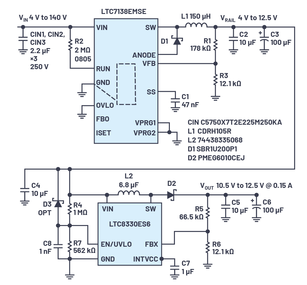 Figure 3: High voltage, dual stage-based circuit electrical schematic where the V IN is 5.0 to 140V and the V OUT is 10.5V at 0.1 to 0.15A.
As long as VI N > 12.5V, the voltage on the output of the boost converter is 12.5V and by far exceeds the preset value of 10.5V, so there’s no switching action in the boost section and only the buck is active.
As the input voltage reduces to the level of 12.5V or below, the buck converter stops switching, but it keeps the internal P-channel MOSFET in the ON state, allowing 100% duty cycle operation.
If input voltage falls below 12.5V, then both voltages, V RAIL (intermediate rail) and V OUT, fall to the V IN level. In the 10.5V < VRAIL < 12.5V range of the intermediate rail, both the converter’s buck and boost do not switch.
If the input voltage continues to fall and the V RAIL level drops below 10.5V, the boost converter becomes operational, keeping V OUT at 10.5V.
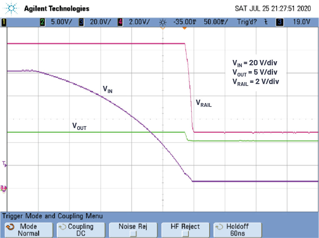
Figure 4: High voltage, dual stage-based bias circuit waveforms. The load current is 0.15A and the time scale is 50ms/div.
The waveforms illustrating the functionality of this converter are presented in Figure 4. The minimum input voltage of 5.5V at the load current is 0.15A. Reducing the load to 0.1A corresponds to a minimum input voltage of 5.0V, as shown in Figure 5. The rise of the input voltage from 5.0 to 100V is illustrated in Figure 6. A photo of the converter is shown in Figure 7.
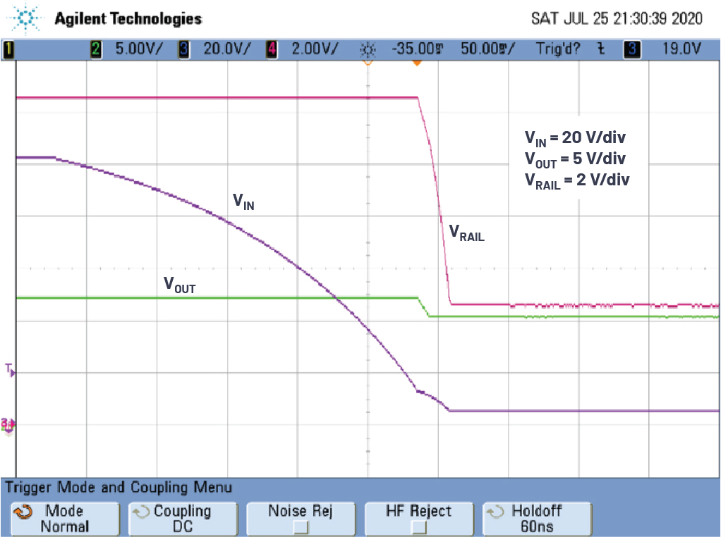
Figure 5: High voltage, dual stage-based bias circuit waveforms. The load current is 0.1A and the time scale is 50ms/div.
Component selection
The maximum input voltage and load currents define the minimum operating input voltage of the boost and correspondingly the minimum input voltage of the entire power supply.
![]()
![]()
Assuming VO, IMAX and IO as given, then the boost minimum voltage can be described as: ![]()
However, if VO, VINMIN, and IMAX are given, the maximum output current IO is: ![]()
It’s important to keep major power systems operational over a wide input voltage range. This article discusses solutions to this goal. The circuits presented here generate the stable bias level at input voltages up to 140V and down to 5.0V during the input voltage droops. A secure bias level guarantees normal functionality of high voltage MOSFETs and control blocks. The proposed schemes using highly integrated converters reduce component count and overall cost. Adjustments can be made to minimize solution height if required by the application.
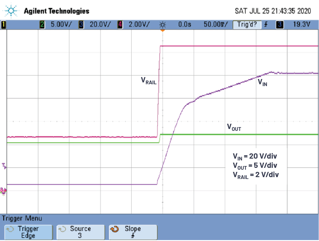
Figure 6: The input voltage rises waveforms. The load current is 0.1A and the time scale is 50ms/div.
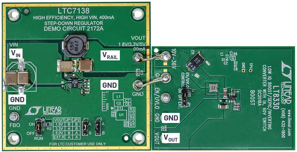
Figure 7: The LTC7138 converter breadboard.