


By Diego de Azcuénaga
The AONK40202 is designed to support high power density in DC/DC conversion applications, incorporating advanced features specifically aligned with the demanding power distribution needs of modern AI servers and data centres.
Peter Wilson, Sr. Director of MOSFET product line at AOS, highlights in an exclusive interview with Electronic Specifier that the Source-Down structure enhances PCB connectivity by providing a larger source contact area.
Advanced features to power distribution
Wilson commented that this DFN3.3×3.3 Source Down Centre Gate package offers benefits compared to standard DFN 3.3×3.3 Drain down such as:
* Very low parasitic inductance
* Better die size to package ratio
* Centre Gate offers more flexible options for PCB layout and easier to parallel devices with less vias
* Large clip for drain to support larger current capability
These new packages are in DC/DC such as 48V power architectures for data centres (Brick Power2).
The AONK40202 MOSFET is capable of sustaining continuous current up to 319A and is rated for a maximum junction temperature of 175°C. “This contributes to improved thermal performance, which supports increased power density and overall energy efficiency,” Wilson underlined.
Providing benefits to designers
The effectiveness of the AONK40202 is the combination of low RDS(on) and low switching losses coupled with advanced silicon and packaging technology. These improvements increase the power density and provide designers with the advanced technologies necessary to utilise PCB space more effectively.
Wilson said that Source-Down structure provides direct path through via to ground plane and Centre Gate has easier for gate routing and paralleling.
The current handling performance is a combination of lower Ohmic technology, low RthJC3(Junction-to-Case thermal resistance), and larger clip to achieve the high current capability.
If the PCB design includes vias for the source area to ground plane then the source area is much larger than traditional DFN3.3×3.3 drain down package. “This large source area coupled with a better thermal path to remove the heat will enable a more efficient design and lower losses compared to a “drain down” configuration,” Wilson claimed.
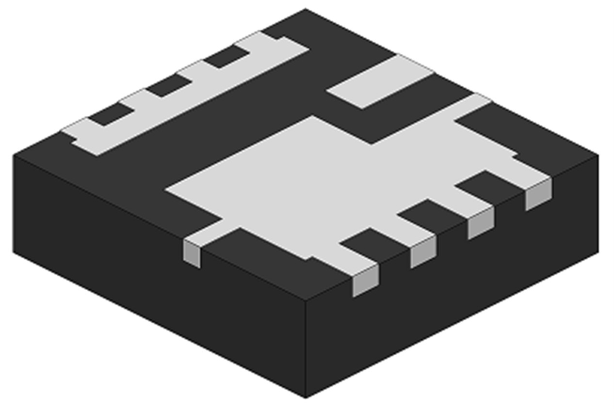
AOS’s AONK 40202 (lead side)
References
1 Alpha and Omega Semiconductor (AOS) is a designer, developer, and global supplier of a broad range of discrete power devices, wide band gap power devices, power management ICs, and modules.
2 A Brick Power, also known as an AC adapter, is an external power supply used with devices like laptops, that converts alternating current (AC) from a wall outlet into direct current (DC) suitable for the device.
3 A low RthJC indicates that the device can dissipate heat from the semiconductor junction to its case more efficiently.