

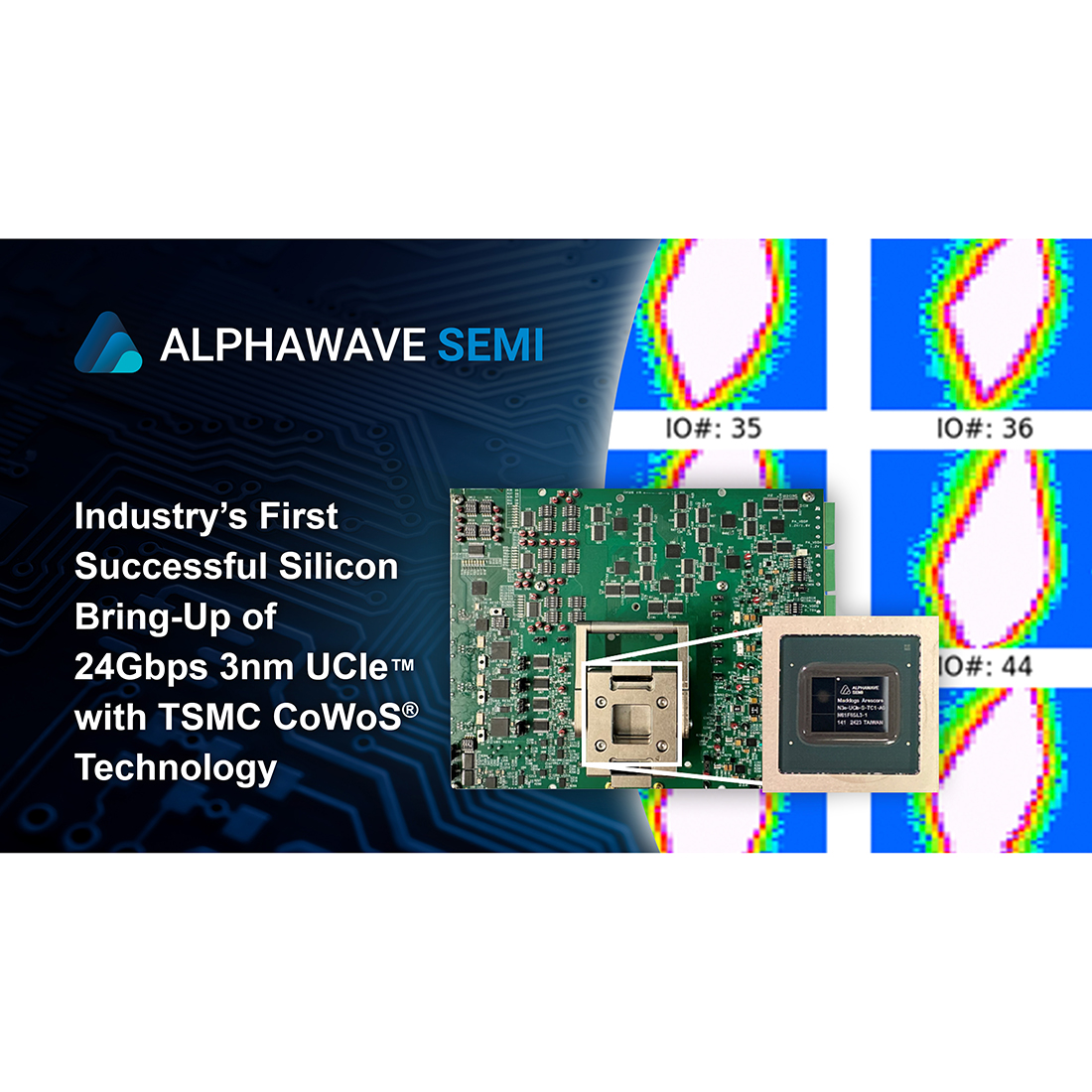
The complete PHY and Controller subsystem was developed in collaboration with TSMC and targets applications such as hyperscaler, high-performance computing (HPC) and artificial intelligence (AI).
Using the foundry’s CoWoS 2.5D silicon-interposer-based packaging, the fully integrated and highly configurable subsystem provides 8 Tbps/mm bandwidth density and reduces I/O complexity, power consumption and latency.
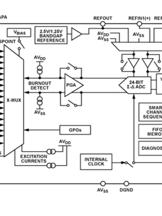
Supporting multiple protocols, including streaming, PCIe, CXL, AXI-4, AXI-S, CXS, and CHI, the IP enables interoperability across the chiplet ecosystem. It also integrates live per-lane health monitoring for enhanced robustness and enables operation at 24 Gbps to give the high bandwidth required for D2D connectivity.
“Achieving successful silicon bring-up of 3nm 24 Gbps UCIe subsystem with TSMC’s advanced packaging is a significant milestone for Alphawave Semi and underscores the company’s expertise in utilising the TSMC 3DFabric ecosystem to deliver top-tier connectivity solutions,” said Mohit Gupta, Alphawave Semi’s SVP and GM, Custom Silicon and IP Gupta also stated the IP sets “a new benchmark in high-performance connectivity solutions.”
Alphawave Semi’s UCIe subsystem IP complies with the latest UCIe Specification Rev 1.1 and includes comprehensive testability and de-bug features such as JTAG, BIST, DFT, and Known Good Die (KGD) capabilities.