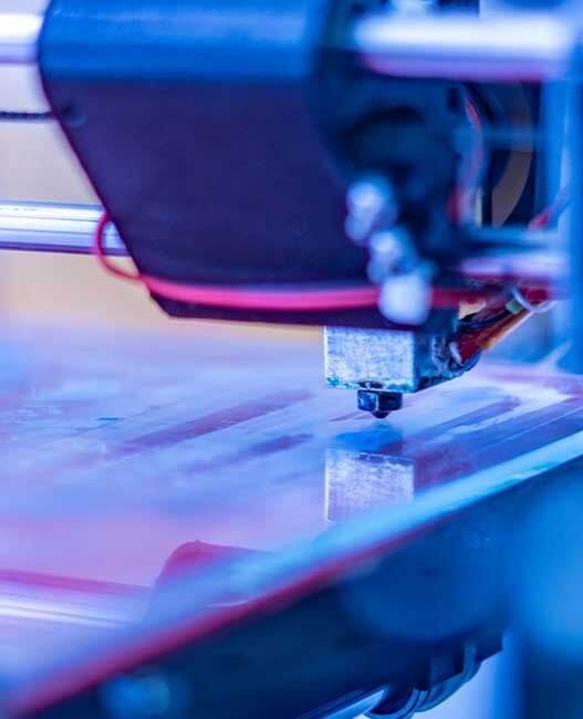




Additive manufacturing has transformed how engineers design and produce 3D printed components for electronic devices. These parts enable intricate geometries and custom configurations beyond traditional manufacturing capabilities.
The same features that make these components valuable require specialised inspection approaches to ensure quality and reliability.
Applications in electronic production
Engineers use 3D printed components to solve design challenges that traditional manufacturing methods struggle to address. Embedded sensors integrate directly into circuit boards and housings during the printing process. Custom substrates can accommodate the unique thermal demands of high-performance processors. Intricate housings protect sensitive electronics while maintaining precise dimensional tolerances for connectors and interfaces.
These applications extend to heat sinks with internal cooling channels that optimise thermal management in compact spaces. Complex geometries tuned to specific frequencies make antenna arrays more effective, while wearable devices benefit from flexible circuits that bend and conform to irregular surfaces. Additive manufacturing offers design freedom that allows engineers to consolidate multiple parts into single assemblies and reduce the overall component count.
Each layer must bond properly to prevent delamination during operation, as internal voids throughout the build can compromise structural integrity. Dimensional accuracy matters when components need to fit precisely with other parts in an assembly. Inspecting these characteristics means using methods tailored specifically to printed parts.
Core obstacles for defect detection
Both traditional and additive production processes can cause invisible defects in the internal structure that lead to spontaneous device failure. Different technologies produce distinct types of flaws. For instance, fused deposition modeling, a method that deposits melted material layer by layer, may create gaps between layers in a component. Selective laser sintering, which uses a laser to fuse powdered material, can trap unmelted powder particles. No single inspection technique detects all potential imperfections.
Complex internal geometries
Printed heat sinks often incorporate internal cooling channels that weave through the component in three dimensions. These channels measure fractions of a millimeter in diameter and follow curved routes that maximise surface area. Traditional non-destructive testing (NDT) tools face significant limitations when inspecting parts with complex geometries, like intricate, curved or sub-millimeter internal pathways without destroying the part.
Tight curves and small openings remain physically inaccessible to contact-based measurement devices, while optical systems need a direct line of sight to capture surface data. A defect hidden within a lattice structure or buried beneath multiple layers will likely escape detection by conventional tools. That said, engineers need alternatives that can penetrate solid materials and map internal features without having to cut parts open.
Surface roughness limitations
The layer-by-layer building process creates surface textures that look and feel different from machined or molded finishes. Each deposited layer leaves a visible line, and this texture changes how measurement tools interact with the part. Surface roughness significantly affects confocal chromatic distance measurements, a noncontact optical method for measuring surface height, and throws off optical or tactile probes trying to capture dimensional data.
Rough surfaces scatter light instead of reflecting it cleanly back to optical sensors. Tactile measurement devices only contact the high points on a surface and can miss the recessed areas between layer lines entirely. This leads to measurement errors that exceed the tight tolerances precision electronics components need. The extent of deviation depends on the probe tip size and the roughness pattern itself.
Modern quality control for 3D printed components
Catching the flaws mentioned above means using specialised inspection tools for 3D printed parts. Conventional measurement systems struggle with complex geometries and rough surfaces, so engineers need more adaptive approaches. The techniques they choose depend on which imperfections matter most and what material they’re inspecting.
Non-destructive evaluation methods
X-ray computed tomography builds three-dimensional images by rotating a component between an X-ray source and a detector array, allowing inspectors to see internal structures without cutting the part open. Hundreds of cross-sectional slices get captured by the system, then reconstruction software assembles them into a complete volumetric model. Internal voids, dimensional variations and material density inconsistencies throughout the entire part become visible with this approach.
Acoustic microscopy uses high-frequency sound waves to detect subsurface flaws and delamination between layers. Interfaces between materials with varying densities reflect the ultrasonic pulses differently.
Infrared thermography monitors how heat flows through a component, helping inspectors identify thermal anomalies that may point to poor layer adhesion or trapped voids. These NDT techniques reveal hidden flaws that standard visual inspections and conventional testing would miss entirely, providing detailed information about what’s happening inside the structure.
Instant defect recognition
Real-time verification spots errors while production is happening instead of finding them later. Pick-and-place machines on electronics assembly lines now capture high-resolution images immediately after picking up a component and before setting it down on a circuit board. Deep learning algorithms then scan these images and flag problems immediately.
This happens in less than five milliseconds on average, which is fast enough to check every single component without slowing anything down. The speed makes 100% inline inspection possible and pulls out visibly defective parts before they get mounted. Manufacturers can catch dimensional errors, surface damage and missing features while components are still moving through the assembly process.
Advancing inspection capabilities
The inspection methods available today address challenges that once limited the adoption of 3D printed components in critical electronics applications.
As detection techniques continue to advance alongside printing technologies, engineers gain confidence to push geometric complexity further and integrate printed parts into more demanding roles where failure can carry serious consequences.