




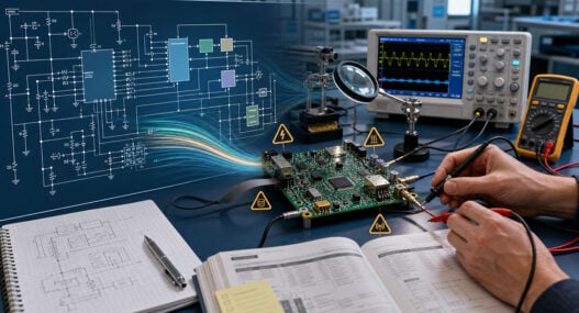
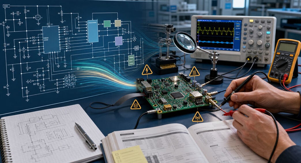
Generating a plausible circuit is becoming faster. Establishing that it satisfies the product brief, component data, and physical constraints remains an engineering task.
Generative AI changes the economics of early-stage circuit design. A product brief can be converted into a block architecture and editable schematic without entering every symbol, net, and component field manually. Yet capture was never the only source of design risk. As it accelerates, more engineering effort moves into requirements interpretation, component validation, and cross-domain verification.
The important question is not whether an AI-generated schematic looks complete, but whether it exposes enough evidence to be challenged. Consider a compact, battery-powered BLE audio recorder specified to capture speech continuously, support ‘real-time transcription’, store audio locally, and synchronise with a phone. Its architecture is credible: a charger and power path, regulated rail, BLE processing, digital microphone, non-volatile storage, antenna, and user I/O. It also shows why architectural plausibility is only the beginning.
A plausible architecture can conceal unresolved requirements
The phrase ‘real-time transcription’ does not identify where transcription occurs. It could mean processing speech on the embedded device, streaming audio to a phone, or forwarding it to a Cloud service. Each interpretation changes the memory, radio throughput, processing load and energy budget. A schematic can connect a microphone, processor, and flash correctly while leaving this core system decision unresolved.
In the design study, an nRF52840 controller interfaces with an SPH9855 PDM microphone and a 1Gbit GD5F1GQ5 QSPI NAND device. Net names such as AUDIO_PDM_CLK, AUDIO_PDM_DATA and STORAGE_QSPI_* make the intended data paths visible. This does not establish that the data path can sustain the required throughput.
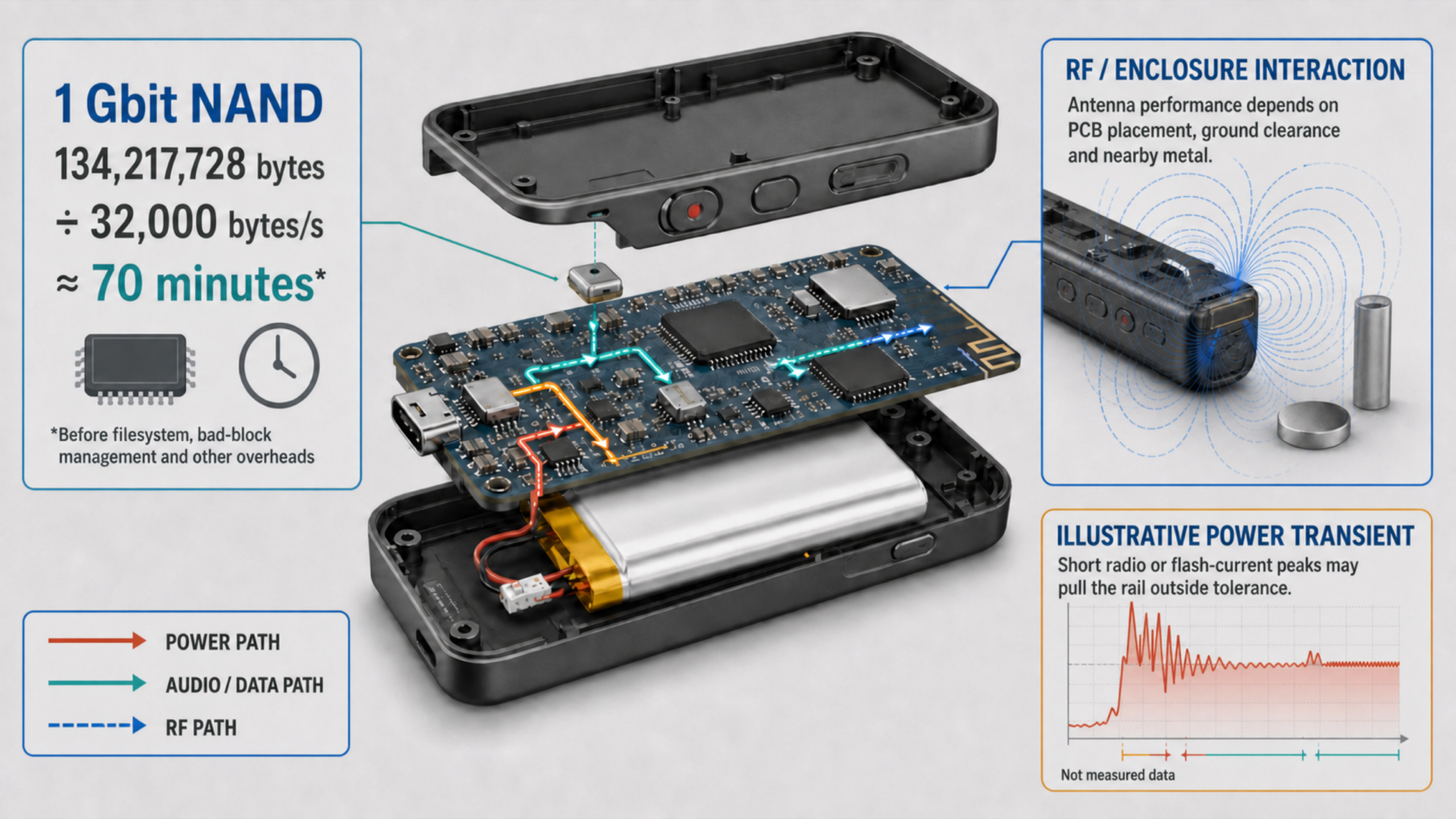
Consider storage duration. A 1Gbit device provides 134,217,728 bytes before filesystem, bad-block management and other overheads. Uncompressed 16kHz, 16-bit mono PCM consumes 32,000 bytes per second, giving a theoretical maximum of about 70 minutes. Compression could extend that time, but would introduce processing, buffering, and firmware-power consequences. The product requirement must therefore specify duration and encoding before storage capacity can be judged adequate.
This is the first verification shift introduced by AI: ambiguity that might once have delayed schematic capture can instead be converted into a concrete but assumption-heavy design. Those assumptions need to become reviewable engineering data, not disappear behind a finished-looking drawing.
Power integrity begins before simulation
The same issue appears in the power tree. The draft uses a BQ21080 charger and power-path device, a DIO7005 load switch, an ST1PS01 1.8V buck regulator and a MAX17048 fuel gauge. The functional split is reasonable, but selecting recognisable parts does not validate the power system.
The review still needs to reconcile battery chemistry and capacity, charge current, USB input behaviour, regulator operating range, rail sequencing, and the peak currents created by radio transmission, flash activity, and audio processing. The average current alone is not enough. A short radio or storage transient may pull the regulated rail outside tolerance even when the spreadsheet energy budget appears comfortable. Capacitor values, inductor selection, current limits, and layout-sensitive switching loops must all be checked against the exact device variants and their primary documentation.
Power-state ownership is equally important. If firmware controls the load switch, the schematic should make the enable polarity, default state, and pull resistance unambiguous. If the fuel gauge shares an I²C bus, the rail domain and pull-ups must remain valid in every sleep and charging state. These are interactions between hardware behaviour and firmware policy; neither an attractive schematic nor an electrical rules check can resolve them automatically.
Component data meets physical design
AI-generated component choices must resolve to exact orderable parts, symbols, and footprints. Package suffixes matter because pin maps, exposed pads, and assembly constraints may differ within a family. The BOM and schematic must agree on manufacturer part number, package variant, footprint, and quantity.
Some of the hardest constraints are only partially represented by connectivity. A PDM microphone needs a valid clock and supply, but acoustic-port orientation and enclosure geometry determine whether it can capture useful audio. A 2.4GHz chip antenna can be connected to an RF feed in the schematic, but its performance depends on the matching network, ground clearance, PCB edge placement, and the final enclosure. A compact product that uses magnets or nearby metal introduces further uncertainty. The antenna therefore requires explicit layout constraints and measurement on hardware.
Similar boundaries exist around USB, programming access, and test points. Circuits may pass logical review while remaining inaccessible after enclosure assembly or unsuitable for production test. Attaching these constraints early makes the generated schematic more valuable.
ERC checks consistency, not intent
Electrical Rules Checking remains necessary. It can identify common connection errors, including unconnected pins, undriven power inputs, and conflicting outputs. However, KiCad’s own documentation makes clear that ERC cannot guarantee that a design will work.
For this recorder, ERC cannot decide whether 70 minutes of theoretical raw storage meets the intended use case. It cannot confirm radio performance inside the enclosure, validate the acoustic path, prove that transient current is acceptable or determine whether firmware can service the data stream while maintaining the required battery life. A clean report is evidence that a defined set of schematic rules has been satisfied; it is not product approval.
The practical output of AI schematic generation should therefore be more than a circuit diagram. It should carry traceable requirements, named assumptions, component specifications, aligned BOM and footprint data, explicit physical constraints, ERC results, a record of open issues, and key risks. This lets engineers separate what has been generated from what has actually been verified.
AI can reduce the effort needed to reach first prototype. Its greater engineering value will come from making uncertainty visible sooner. The bottleneck has not disappeared; it has moved from drawing the circuit to proving that the circuit represents the intended product.