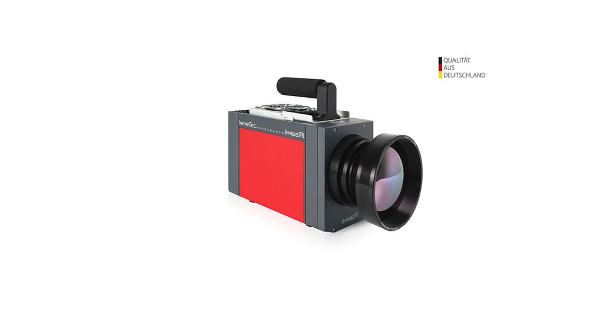


InfraTec’s E-LIT automated test solution provides high-fidelity inspection for advanced electronic and semiconductor modules using high-sensitivity lock-in thermography. This modular system reliably identifies and localises thermal anomalies, ensuring the integrity of complex multilayer PCBs and multi-chip modules.
Introduction
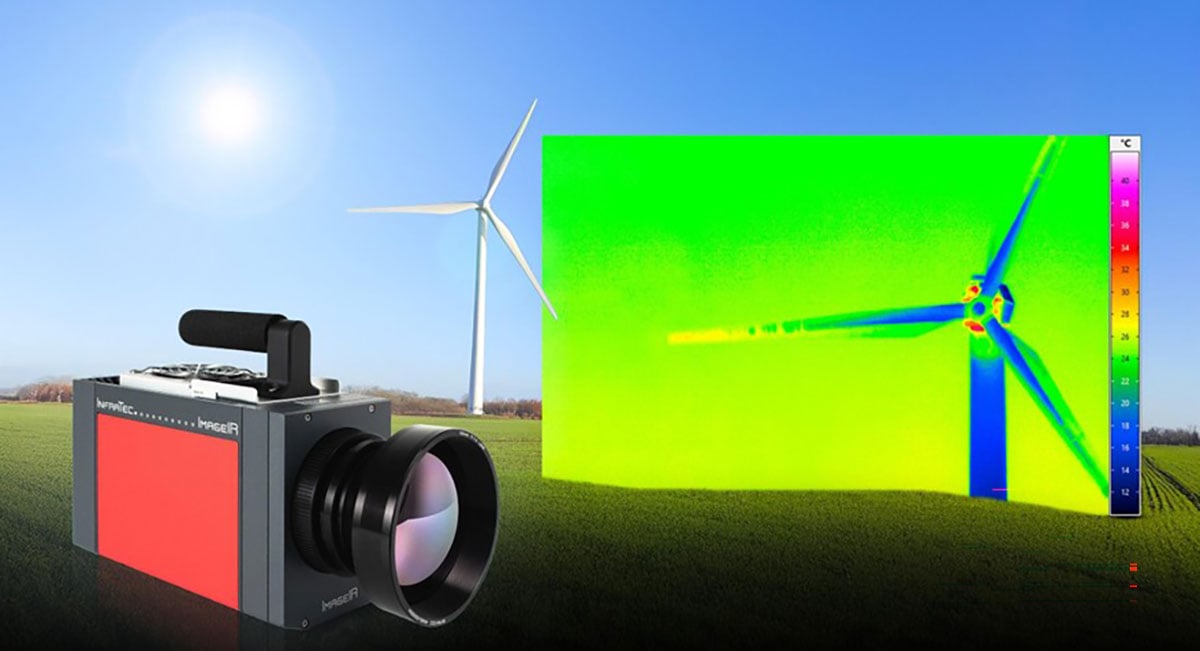
Thermographic inspection with infrared cameras enables non-contact, real-time analysis of electronic systems for failure detection, thermal design validation, and quality assurance. It helps engineers identify hotspots caused by contact resistance, cable constrictions, hidden cracks, soldering defects, and even short circuits within multilayer boards. The technology also reveals power losses from high-frequency mismatch and supports evaluation of cooling concepts, heat sink connections, and board layouts to reduce component aging. Beyond diagnostics, thermography is used to assess service life under load cycles and troubleshoot power electronics such as inverters and charging stations. A newer application is the detection of thermally active watermarks, which can expose unauthorised hardware changes or malicious modifications by tracking a chip’s thermal fingerprint.
Modular automated test bench
The E-LIT test bench, especially designed for the analysis of electronic components, delivers the following strategic advantages for semiconductor inspection:
High-precision thermal analysis and failure analysis
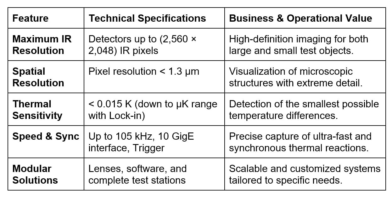
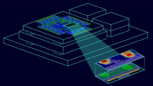
This modular test bench is designed for advanced thermal analysis of electronic and semiconductor devices using online lock-in measurement techniques. The system enables extremely sensitive temperature monitoring, achieving reliable detection of thermal anomalies in the mK and μK ranges. Due to this high sensitivity, it is possible to spatially locate critical defects such as point and line shunts, oxide defects, and transistor or diode failures. This works even inside complex structures like multilayer PCBs and multi-chip modules, because the inspection depth can be precisely controlled via the excitation frequency.
Authenticity and detection flexibility
Beyond fault localisation and analysis, the system enables the detection of ‘watermarks’ and specific thermal signatures, which are essential for component authenticity analysis and anti-counterfeiting measures. To meet diverse inspection needs, the test bench integrates versatile thermographic systems that can utilise both cooled and uncooled detectors, ensuring optimal data capture based on specific resolution and speed requirements.
Specialised software and laboratory quality control
System operability is managed via the IRBIS 3 active software, a tool optimised for chip testing that offers comprehensive analysis options under laboratory conditions. This software facilitates the interpretation of complex data and the generation of detailed technical reports, allowing quality engineers to validate the structural integrity and thermal behaviour of semiconductors under rigorous and controlled testing environments.
Unified failure analysis and high-resolution microscopy
The E-LIT test bench offers a comprehensive solution for IC failure analysis within a single workstation, bridging the gap from full circuit board overviews to microscopic detail. By utilising specialised microscope lenses, the system achieves a geometric resolution of 1.3 μm per pixel, enabling exhaustive and detailed analysis of chips. This precision is complemented by an online lock-in measurement capability that provides thermal resolution in the microkelvin range, ensuring the highest sensitivity for detecting even the most subtle thermal anomalies.
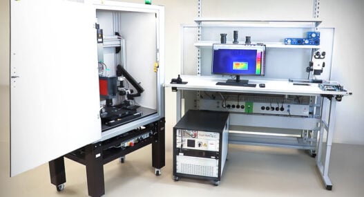
Customisable modular design and operational flexibility
Engineered for adaptability, the test bench features a customised modular station equipped with manual or motorised X-Y tables and adjustable Z-axes. This configuration allows for high-precision positioning and automated scanning of larger samples, ensuring optimal working distances for objects of any size. Furthermore, the system’s flexibility is enhanced by interchangeable components, including various optics, specialised specimen holders, and versatile contacting options to meet specific testing requirements.
Integrated high-voltage testing and characterisation
For power electronic applications, the platform integrates a high-voltage test station supporting source meter units up to 3kV. The setup includes a mandatory contact protection system and operating status indicator lights to ensure maximum safety during high-stress tests. Additionally, an integrated IV curve tracer allows for precise i-v characterisation, providing engineers with a complete diagnostic toolset to validate device performance and reliability under real-world electrical conditions.
IRBIS 3 active: thermographic software for semiconductor analysis
The IRBIS 3 active software serves as a comprehensive operational platform tailored for rigorous laboratory environments. It features an intuitive user interface that simplifies complex diagnostic tasks, including real-time visualisation of electronic components across various operational states. A key highlight is the automated failure classification add-on, which categorises defects based on user-defined parameters. To accommodate large-scale testing, the system provides multifaceted storage options for both raw image data and detailed measurement results.
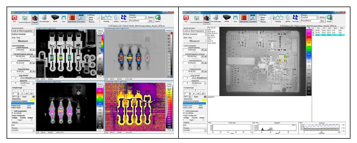
Advanced imaging capabilities allow users to represent complex intensity information through 0°, 90°, or customised phase angle settings, as well as the ability to merge live and amplitude images for better clarity. For specialised needs, the software can be expanded with optional modules such as drift compensation, IV and power loss measurement, and DC-mode. Furthermore, it supports professional integration through dedicated user administration protocols and standard interfaces like Profibus and Ethernet.
Case study: fault isolation on chips and power modules at STM
STMicroelectronics, a global specialist in European semiconductor manufacturing, utilises the InfraTec E-LIT system for comprehensive fault analysis across its product lines – including chips, sensors, and power modules. The system is highly valued by users for its versatility and its ability to provide clear visual identification of defects.
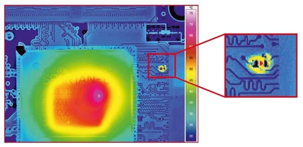
The E-LIT solution utilises Lock-in thermography to pinpoint local defects by detecting thermal anomalies. This process works by applying a specific electrical excitation to an electronic component or assembly, allowing the system to identify and analyse irregularities based on their heat signature.
At STMicroelectronics, this failure analysis setup was integrated into its laboratory with a comprehensive hardware suite, including an infrared camera with adjustable positioning, an X-Y table, and specialised lenses. To further improve functionality, the system was enhanced with a binocular, facilitating the precise connection of power supply contacts to the components under test.
By utilising high-end ImageIR series infrared cameras, surface temperature changes are monitored during electrical activation to locate specific ‘hot spots’. This technology enables the detection of minute thermal anomalies in the millikelvin (mK) or microkelvin (μK) range, making it possible to identify critical defects such as point and line short circuits, oxidation, and internal faults in transistors or diodes.
The E-LIT system offers versatile imaging through 25mm wide-field lenses and microscope lenses that resolve details down to 1.3 µm. It achieves exceptional sensitivity, detecting chip-level hot spots at just 2 μA while supporting power module excitation up to 3kV.
Analysis is managed via IRBIS 3 software, utilising specialised colour palettes and inverted modes to streamline fault detection. This performance is further optimised through a collaborative feedback loop, where user insights drive continuous system updates and faster diagnostic results from InfraTec.
At STMicroelectronics, lock-in thermography stands as a primary technique for diagnosing electrical component failures. This intuitive approach excels at pinpointing the exact location of short circuits and other irregularities. Notably, the E-LIT solution was instrumental in securing approval for a new mass production project in Calamba, enabling the team to rapidly identify hot spots across numerous batches.
InfraTec E-LIT solution: high-precision infrared thermography for electronics