
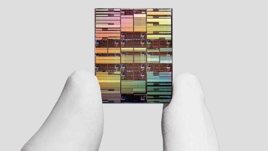


Alphawave Semi has announced the successful tape-out of its latest ultra-high-speed connectivity technology, marking a major step forward in three-dimensional chiplet integration for advanced computing.
The London- and Toronto-listed semiconductor designer said its new UCIe 3D intellectual property (IP) had been successfully produced using Taiwan Semiconductor Manufacturing Company’s (TSMC) SoIC-X technology, part of the foundry’s advanced 3DFabric platform.
The development underscores Alphawave Semi’s ambitions to strengthen its position in the growing market for chiplet-based architectures, which are expected to play a central role in powering next-generation data centre, artificial intelligence (AI), and high-performance computing (HPC) systems.
By adopting TSMC’s SoIC-X packaging — a cutting-edge form of 3D die stacking — Alphawave Semi said it achieved a tenfold improvement in power efficiency compared with conventional 2.5D interfaces, as well as up to a fivefold increase in signal density.
“With the growing complexity of AI models, traditional scaling driven by Moore’s Law is no longer sufficient,” said Mohit Gupta, Alphawave Semi’s Executive Vice President and General Manager. “By combining our high-speed 3D UCIe IP with TSMC’s SoIC-X technology, we are directly addressing the bandwidth and memory bottlenecks that limit next-generation AI and HPC systems.”
The company said its 5nm UCIe-3D base die supports through-silicon vias (TSVs) to deliver power and grounding to a 3nm top die, improving energy efficiency and performance. Its proprietary 3DIO design flow also aims to accelerate the construction and verification of 3D chip stacks.
Aveek Sarkar, Director of Ecosystem and Alliance Management at TSMC, said Alphawave Semi’s work on the SoIC-X platform illustrated how collaboration within TSMC’s Open Innovation Platform (OIP) ecosystem was helping customers “push the envelope of product innovation” through more efficient and powerful AI systems.
The announcement follows Alphawave Semi’s June milestone, when it completed the tape-out of its UCIe IP on TSMC’s 2nm process using 2.5D CoWoS technology. The company is now developing next-generation UCIe solutions supporting 64G data rates, as it seeks to maintain its momentum in the rapidly evolving chiplet-based computing landscape.
Earlier this year Siemens Digital Industries Software announced it has signed an exclusive OEM agreement for its EDA business to bring Alphawave Semi’s portfolio of high-speed interconnect silicon IP to market through its sales channel.
Juan C. Rey, Senior Vice President and General Manager of the Calibre product line at Siemens Digital Industries Software, said the collaboration between Alphawave Semi and Siemens reflected a “shared vision” for delivering advanced 3D design and verification tools. The partnership allows early analysis of key electrical and thermal parameters in next-generation IC systems, he added.