


What is a silicon chip? A silicon chip, also known as a semiconductor chip, is a small piece of silicon wafer embedded with an integrated circuit (IC), designed to process or store data. The main types of silicon chips can be understood in three categories: memory, logic, and discrete and analog. These include microprocessors and memory chips.
A brief history
Silicon is now a material at the heart of a billion-dollar semiconductor industry. The history of silicon chips maps the rise of electronics and their permeation into every aspect of modern life: from modern computing to cars and smartphones.
The history of semiconductor chips can be traced back to 1947, when Walter Brattian, William Shockley, and John Bardeen at Bell Laboratories invented the point-contact transistor, which was a big step towards the creation of the semiconductor. By 1954, Texas Instruments (TI) had commercialised the first silicon transistor, where the company took advantage of silicon’s thermal properties. By 1958, Jack Kilby, while working at TI, developed the first monolithic integrated circuit (IC).
This anticipated a transition from using germanium to silicon, which took place in the 1960s, as the semiconductor material of choice. Silicon chips replaced components in radios, calculators, and eventually computers.
By 1965 Gordon Moore coined the well-known Moore’s Law: predicting that the number of transistors on a chip was doubling roughly every two years.
Semiconductor manufacturing became a global enterprise as companies based in Japan, South Korea, and Taiwan all invested heavily in foundries.
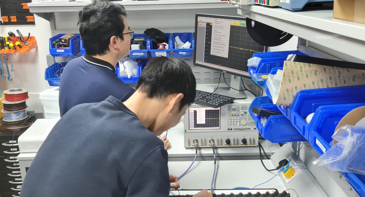
Today, silicon chips are indispensable, and the 2020-2023 global chip shortage demonstrated just how important these chips are for powering the technologies we have come to depend on, triggering the implementation of regulation such as the US CHIPS and Science Act and the European Chips Act.
How are silicon chips made?
The semiconductor manufacturing process creates silicon chips, and can be understood by being split up into 6 key steps:
- Wafer preparation and fabrication: the silicon wafer is cleaned, polished, and prepared as a substrate
- Patterning (photolithography): a pattern is created on the silicon wafer using a process known as photolithography
- Doping: impurities are added to the wafer to change its electrical properties, with the most common types of impurity used including boron or phosphorus
- Deposition: thin films of material are deposited on the wafer to create the electronic components and is achieved using a variety of techniques such as chemical vapor deposition
- Etching: material is removed from the wafer’s surface to create the right shape and structure for the electronic components, using wet etching, dry etching, and plasma etching
- Packaging: finally, the electronic components are packaged into a final product
Generally speaking, the entire wafer fabrication process can take from 16 to 18 weeks, while the process of creating a chip will take from several weeks to several months.
Advancements in silicon chips
Existing constraints facing silicon chips – like physical scaling, power density, memory bottlenecks, and rising fabrication costs – have fuelled advancements that have sought not only to address these constraints, but to make the chips faster, smaller, and more powerful.
US semiconductor companies reportedly invest about one-fifth of their total revenue in R&D, a consistent prioritisation in silicon development that demonstrates not only how important chips are today, but how important a competitive edge is for these companies.
For instance, Moore’s Law has resulted in challenges around power density and heat dissipation. Thermal hotspots can affect reliability, performance, and complicate system-level cooling. The use of Dynamic Voltage and Frequency Scaling (DVFS) and adaptive power management techniques have sought to address this, as well as the integration of on-die thermal sensors and machine learning algorithms to optimise runtime.
Memory bottlenecks, meanwhile, are being tackled with the application of High Bandwidth Memory (HBM) and 3D-stacked DRAM (architecture where multiple DRAM dies are stacked on top of one another) to reduce latency and increase throughput.
Rising fabrication costs can be attributed to silicon processes like 3nm, which are comparatively more expensive to manufacture than 5nm or 7nm because of the process complexity, lithography tooling, and yield challenges. The chiplet approach allows designers to mix and match IP blocks from different nodes which subsequently reduces reliance on single-die monolithic integration; and advanced packaging allows for heterogeneous integration which lowers the cost of scaling performance.
Conclusion
Our dependence on silicon chips to run our cars, computers and smartphones is due to the particular advantages silicon provides; namely its unique electrical properties but also its thermal conductivity and wide availability. The investment, time and resources companies put into semiconductor development has led to several advancements which have resulted in more powerful, compact, efficient silicon chips.