ASMPT will be exhibiting at the ECOC 2025 Exhibition, a trade fair for optical communication, running 29 September to 1 October in Copenhagen.
At its booth, it will showcase forward-looking technologies for silicon photonics and co-packaged optics (CPO). The premier of the MEGA-P multi-chip bonder will be a highlight at the ASMPT booth,
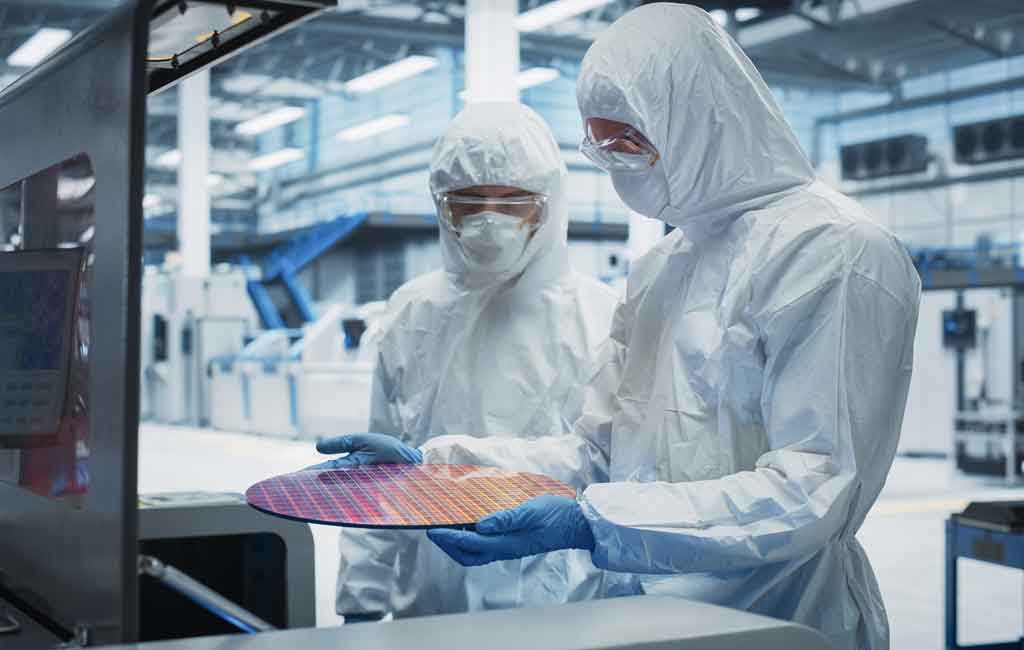
With its long-standing experience in interconnect technologies and its deep-rooted understanding of the challenges in optoelectronics manufacturing, ASMPT provides powerful answers to the growing need for the efficient integration of optical components, especially with regard to applications like high-speed data transmission, data centers, and future AI infrastructures.
MEGA-P: high-precision multi-chip packaging
At ECOC 2025, ASMPT will unveil its new MEGA-P platform: a versatile solution for the precise and efficient packaging of complex multi-chop modules in the areas of photonics, sensor technology, and optical communication.
Due to its modular architecture, the MEGA-P combines a wide range of processes in a single system, including the application of adhesives, 3D post-dispense inspection, and a ‘look-through’ bond head for maximum precision and UV curing. This allows even complex designs to be implemented flexibly and efficiently, for instance in applications that require the integration of lenses or photonic components.
With its intelligent process architecture and integrated automation, the MEGA-P combines several previously separate machine functions while maintaining high precision and adaptability. Users benefit from faster setups, more throughput and maximum flexibility in the face of changing requirements.
“The complexity of modern semiconductors poses new challenges, particularly where bonding technology is concerned,” said Dr. Johann Weinhändler, Regional Head ASMPT Semiconductor Solutions and CEO of ASMPT AMICRA. “With the MEGA-P platform we have created a solution for tasks that previously required a complete machine line while delivering maximum flexibility thanks to its modular design.”
Solutions for co-packaged optics
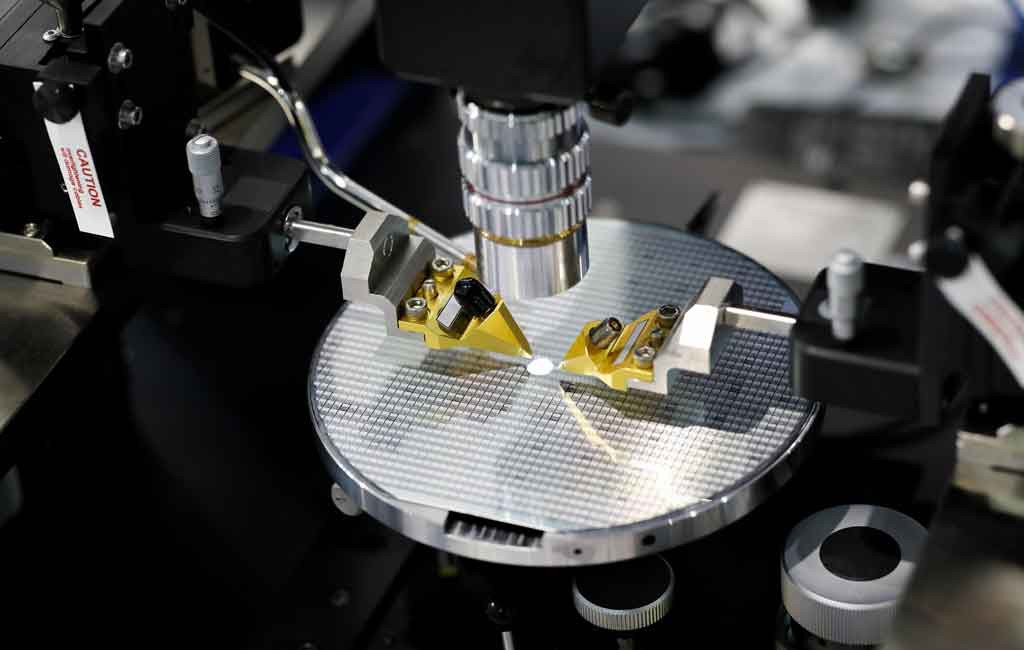
At the ASMPT booth, attendees can learn about high-precision manufacturing solutions for co-packaged optics, including the AMICRA NANO and AMICRA NOVA Pro systems, each of which is tailored to different requirements in optoelectronics integration.
The AMICRA NANO is engineered for the greatest placement accuracy, making it well suited for research, prototyping and complex development projects. It enables the reliable processing of the finest structures and supports modern hybrid bonding processes for applications like the precise integration of photonics and electronics in the smallest of spaces.
The AMICRA NOVA Pro is designed for volume-oriented production. It features high processing speeds paired with high precision, making it particularly suitable for advanced packaging applications. With its automation and flexible material processing capabilities, it makes the mass production of photonics more flexible and scalable.