


This post is about structure, parameters and properties of JFET transistor.
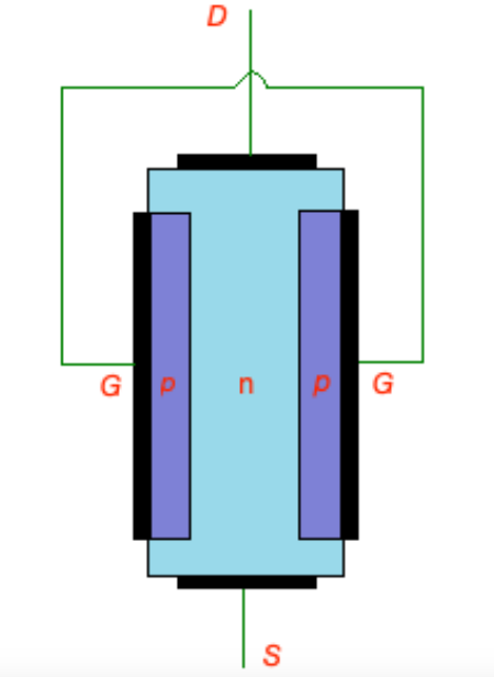
JFET transistor is a three-terminal device, where one of the terminal can control current between two others. JFET transistor terminals are drain (D), source (S) and gate (G). Here current between D and S can be controlled by gate-source voltage.
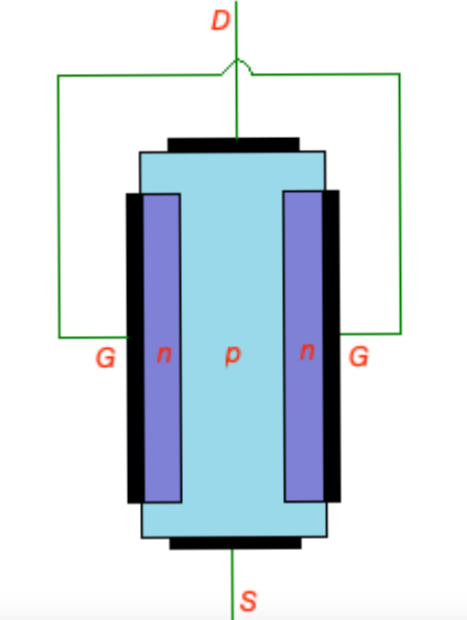
Construction of JFET transistor is depicted on the figure below. N-type JFET transistor consist of n-type semiconductor with heavily doped p-type regions as shown on the figure. P-type areas are forming the gate, both p-type areas and n-type area are equipped with thin contacts layers.
JFET n-type |
JFET p-type |
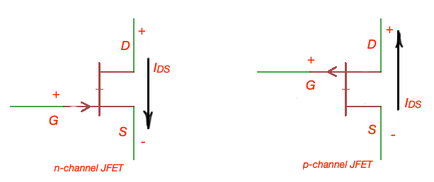
JFET electrical symbols
Let’s consider n-type JFET transistor. Here n-type semiconductor is connected to drain and source with ohmic contacts, p-type semiconductors are connected to the gate and connected to each other.
JFET transistor is in cut-off mode, and does not conduct any current when both source-gate and drain-source potentials are zero. There is thin depletion regions are formed around p-type regions of JFET. Depletion regions are free from free careers, so there is no current through depletion area.
Let’s keep
and apply drain-source voltage
. Current
will flow from drain and source (note that electrons will move in the opposite direction). Here JFET transistor operates in ohmic mode. Depletion region around p-type areas is wider close to drain because of the voltage distribution between drain and source. When
is growing, width of depletion areas close of drain is growing as well. At some point drain-source voltage will reach
level, when these depletion areas will get very close to each other.
voltage is called pinch-off voltage. After this point JFET transistor will go to the saturation mode. Here small channel between two depletion areas will still exist with constant current through is
.
If
, depletion regions still grows around p-type areas of JFET transistor. In order to maintain depletion regions
should be smaller than
. Lower
. lower pinch-off voltage
. Finally when
,
. JFET is off.
 |
 Ohmic mode |

Saturation mode
When JFET transistor operates in ohmic mode, the resistance of n-channel can be controlled by
voltage, so JFET behaves like a voltage-controlled resistor. First approximation of JFET resistance in this case is
.
Finally equations, describing JFET transistor behaviour are:
for cut-off region;
for breakdown voltage;
,
,
for ohmic region;
for saturation region. Here
is a maximum current, when
and
.
If
,
.
If
, then
.
JFET transistor transfer function
Transfer characteristic is the relation between output current
and controlling voltage
. The easiest way to obtain transfer characteristic is to apply Shockley equation
. It gives us
when
and
, when
. Here we are having important relationship between
and
is
.
In order to outline the transfer function, we must calculate
current for different key levels of
.
Transfer function can be obtained from the
characteristics like on the figure below.

Fixed-bias JFET configuration
Three most important relationships for operation of FET transistor devices are
and Shockley equation
.
Here
and
are ac levels.

,
,
, because
.
.
Self-biased JFET transistor configuration

Here
, and from the other side
,
then
and
.
,
In accordance to Shockley equation
, then we are having second order equation that will lead us to quadratic function.