


The objective of this activity is to investigate the frequency response of the common emitter amplifier configuration using an NPN BJT transistor.
Common emitter amplifier topology
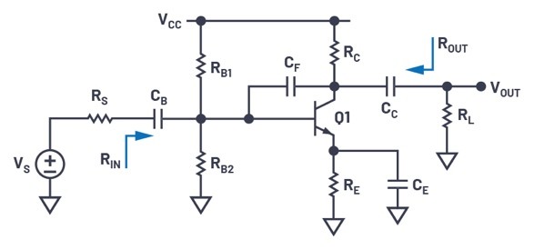
The schematic of a typical common emitter amplifier is shown in Figure 1. Capacitors CB and CC are used to block the amplifier dc bias point from the input and output (ac coupling). Capacitor CE is an ac bypass capacitor used to establish a low frequency ac ground at the emitter of Q1. Miller capacitor CF is a small capacitance that will be used to control the high frequency 3dB response of the amplifier.
Low frequency response
Figure 2 shows the low frequency, small signal equivalent circuit of the amplifier. Note that CF is ignored since it is assumed that its impedance at these frequencies is very high. RB is the parallel combination of RB1 and RB2.
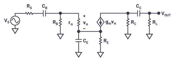
Using short-circuit time constant analysis, the lower 3dB frequency (ωL) can be found as:
High frequency response
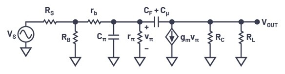
Figure 3 shows the high frequency, small signal equivalent circuit of the amplifier. At high frequencies, CB, CC, and CE can be replaced with short circuits since their impedance becomes very small compared to RS, RL, and RE.
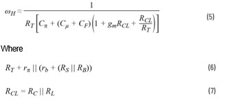
The higher 3dB frequency (ωH) can be derived as:
Thus, if we assume that the common emitter amplifier is properly characterised by these dominant low and high frequency poles, then the frequency response of the amplifier can be approximated by:
Where:
s is the complex angular frequency
AV is the mid-band gain
ωL is the low corner angular frequency
ωH is the high corner angular frequency
Pre-lab setup
Assuming CB = CC = CE = 1 farad and CF = CΠ = Cµ = 0, and, using a 2N3904 transistor, design a common emitter amplifier with the following specifications:
VCC = 5V
RS = 50Ω
RL = 1kΩ
RIN >250Ω
ISUPPLY <8mA
AV >50
Peak-to-peak unclipped output swing >3V
- Show all your calculations, design procedure, and final component values
- Verify your results using the LTspice circuit simulator. Submit all necessary simulation plots showing that the specifications are satisfied. Also provide the circuit schematic with dc bias points annotated
- Using LTspice, find the higher 3dB frequency (fH) while CF = 0
- Determine Cπ, Cµ, and rb of the transistor from the simulated operating point data. Calculate fH using the equation from the High Frequency Response section and compare it with the simulation result obtained in Step 3. Remember that the equation gives you the radian frequency and you need to convert to Hz
- Calculate the value of CF to have fH = 5kHz. Simulate the circuit to verify your result and adjust the value of CF if necessary
- Calculate CB, CC, CE to have fL = 500Hz. Simulate the circuit to verify your result and adjust the values of capacitors if necessary
Lab procedure
The objective of this section of the lab activity is to validate your pre-lab design values by building the actual circuit and measuring its frequency response performance.
Materials:
- ADALM2000 active learning module
- Solderless breadboard
- Six resistors, various values, from the ADALP2000 analogue parts kit
- Four capacitors, various values, from the ADALP2000 analogue parts kit
- One small signal NPN transistor (2N3904)
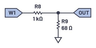
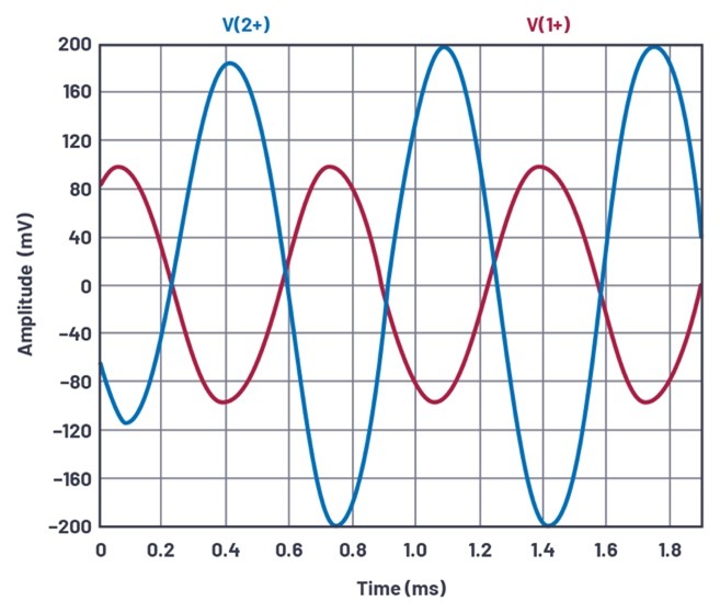
Note that on the source resistor, RS, and the AWG output of the ADALM2000, the AWG output has a 50Ω series output resistance and you will need to include it, along with the external resistance, in series with its output. Also, due to the relatively high gain of your design, you will need an input signal with a small amplitude of around 100mV peak-to-peak. Rather than turning down the AWG in software, it would be better from a noise point of view to insert a resistor voltage divider between the AWG output and your circuit input to attenuate the signal. Using something like the setup shown in Figure 4 will provide both an attenuation factor of 1/16 and a 60Ω equivalent source resistance. Other combinations of resistor values are also possible based on what you have available – in our case, a standard resistor value will be used – 68Ω.
Hardware setup

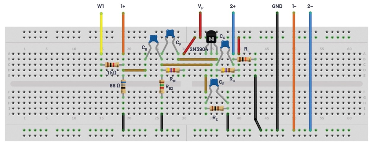
Construct the circuit on your breadboard.
Directions
- Construct the amplifier, based on the schematic in Figure 1, you designed in the pre-lab. Based on your design values from the pre-lab, use the closest standard value from your kit. Remember that you can combine the standard values in series or parallel to get a combined value closer to your design number
- Check your dc operating point by measuring IC, VE, VC, and VB. If any dc bias value is significantly different than the one obtained from simulation, modify your circuit to get the desired dc bias before moving onto the next step
- Measure ISUPPLY
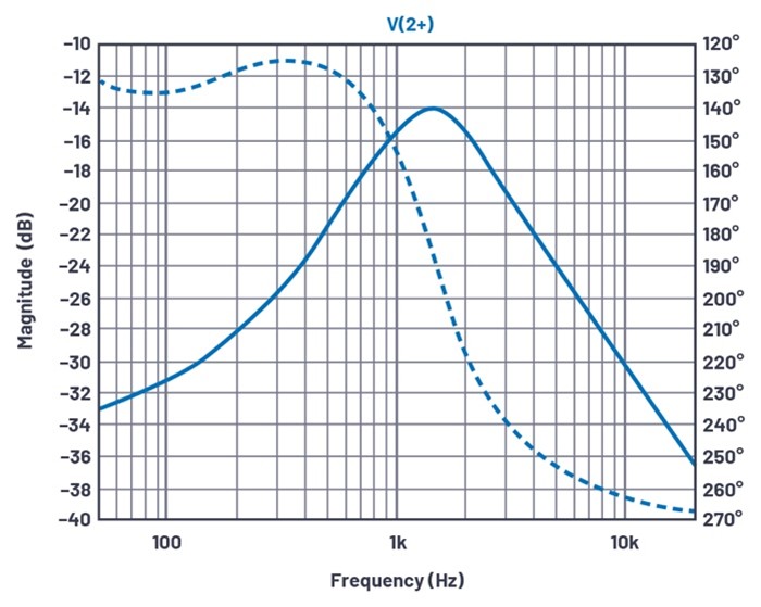
- Use the network analyser instrument in the Scopy software to obtain the magnitude of the frequency response of the amplifier from 50Hz to 20kHz and determine the lower and upper 3dB frequencies fL and fH
- At mid-band frequencies, measure AV, RIN, and ROUT
Plot examples are provided using the LTspice simulations of the circuit in Figure 5.
Question
Replace capacitor CF with a smaller value (0.01µF) and re-measure the response curve with the network analyser instrument or ac sweep simulation. Explain the effect of the new capacitor value in the response that you see.
You can find the answer at the StudentZone blog.
About the authors:
Doug Mercer received his B.S.E.E. degree from Rensselaer Polytechnic Institute (RPI) in 1977. Since joining Analog Devices in 1977, he has contributed directly or indirectly to more than 30 data converter products and he holds 13 patents. He was appointed to the position of ADI Fellow in 1995. In 2009, he transitioned from full-time work and has continued consulting at ADI as a Fellow Emeritus contributing to the Active Learning Program. In 2016 he was named Engineer in Residence within the ECSE department at RPI. He can be reached at doug.mercer@analog.com.
Antoniu Miclaus is a system applications engineer at Analog Devices, where he works on ADI academic programs, as well as embedded software for Circuits from the Lab, QA automation, and process management. He started working at Analog Devices in February 2017 in Cluj-Napoca, Romania. He is currently an M.Sc. student in the software engineering master’s program at Babes-Bolyai University and he has a B.Eng. in electronics and telecommunications from Technical University of Cluj-Napoca. He can be reached at antoniu.miclaus@analog.com.