


ADALM2000 activity: common emitter amplifier
Objective
The purpose of this activity is to investigate the common emitter configuration of the bipolar junction transistor (BJT).
Background
The common emitter amplifier is one of three basic single-stage amplifier topologies. The BJT version functions as an inverting voltage amplifier. The base terminal of the transistor serves as the input, the collector is the output, and the emitter is common to both input and output (it may be tied to the ground reference or the power supply rail), which gives rise to its common name.
Materials
- ADALM2000 active learning module
- Solderless breadboard
- Five resistors
- One 50kΩ variable resistor, potentiometer
- One small signal NPN transistor (2N3904)
Directions
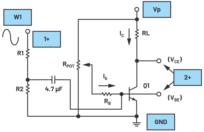
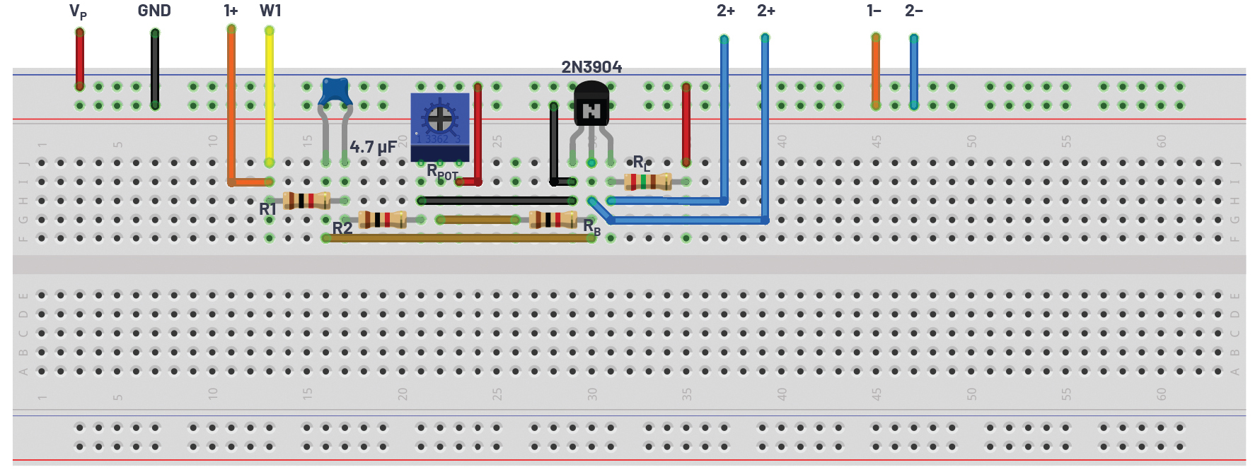
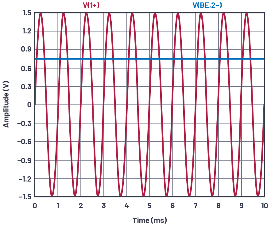
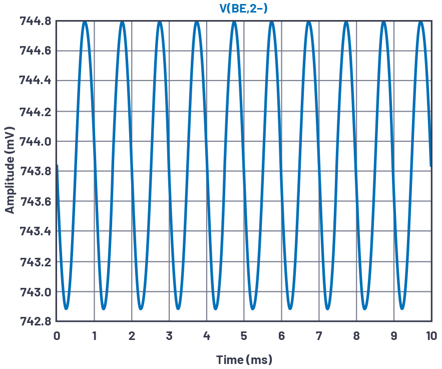
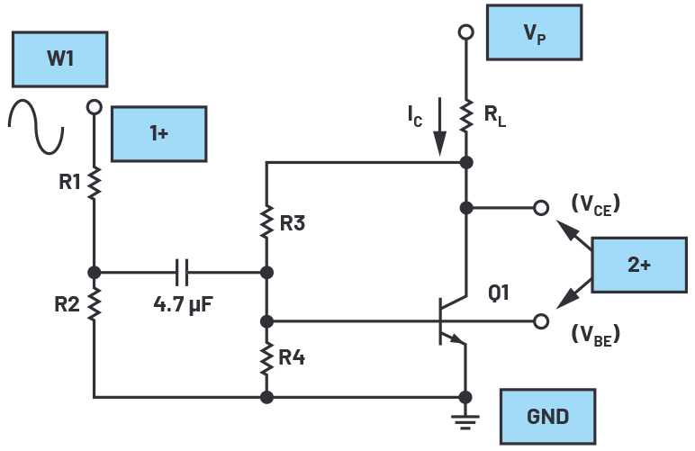
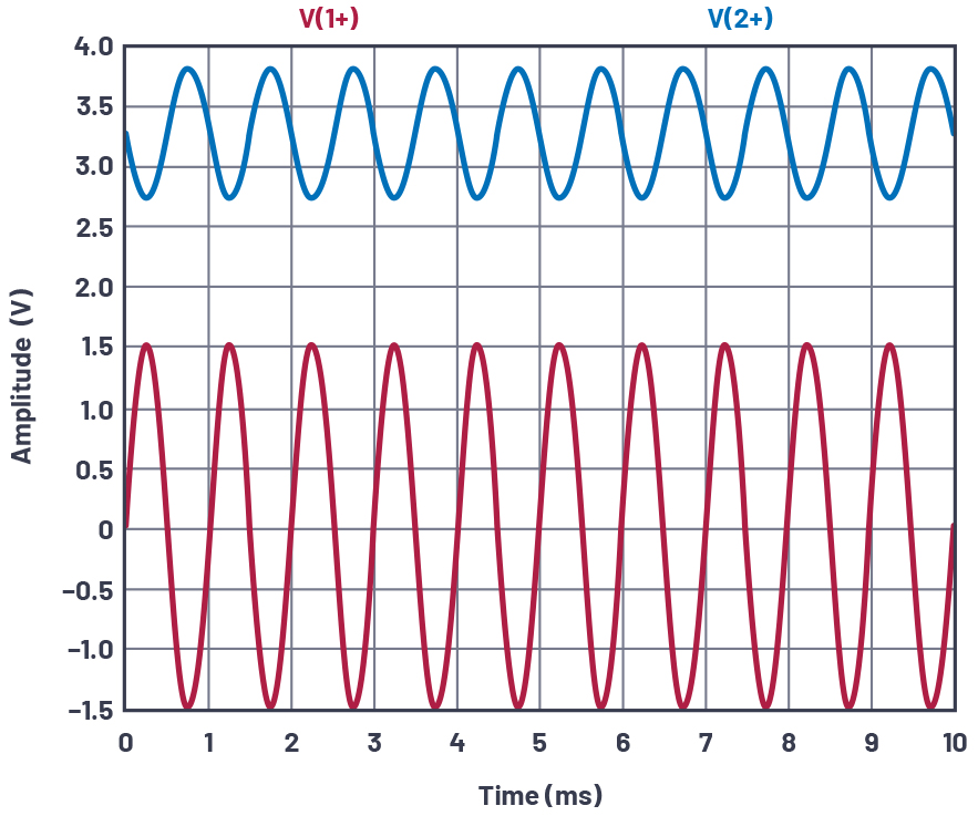
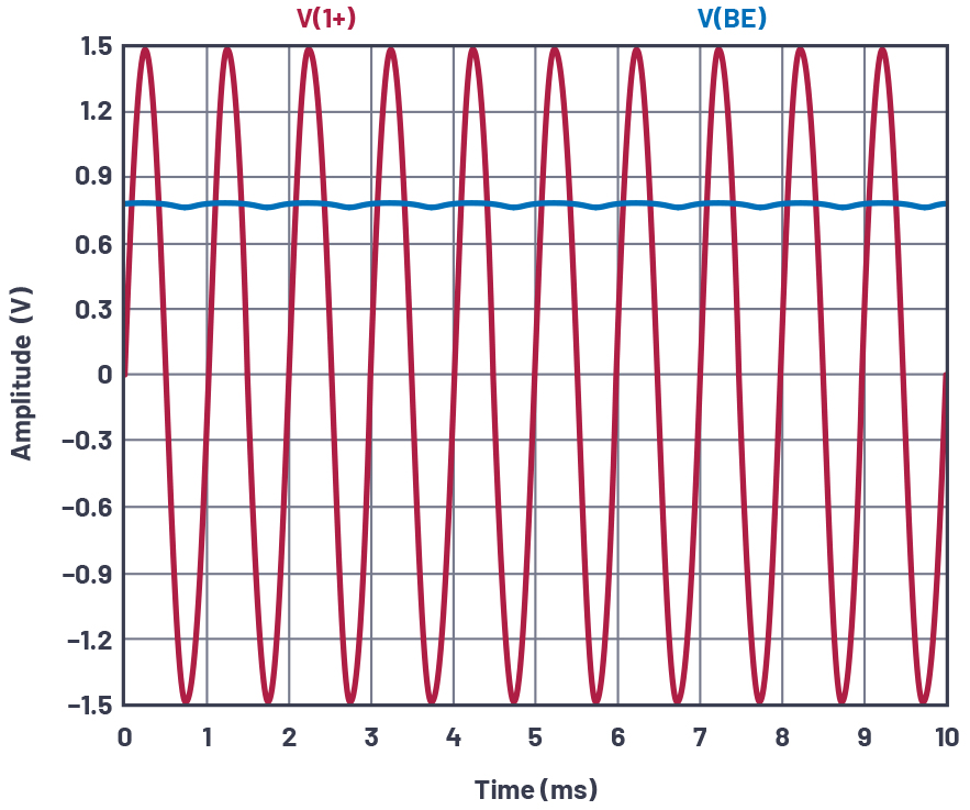
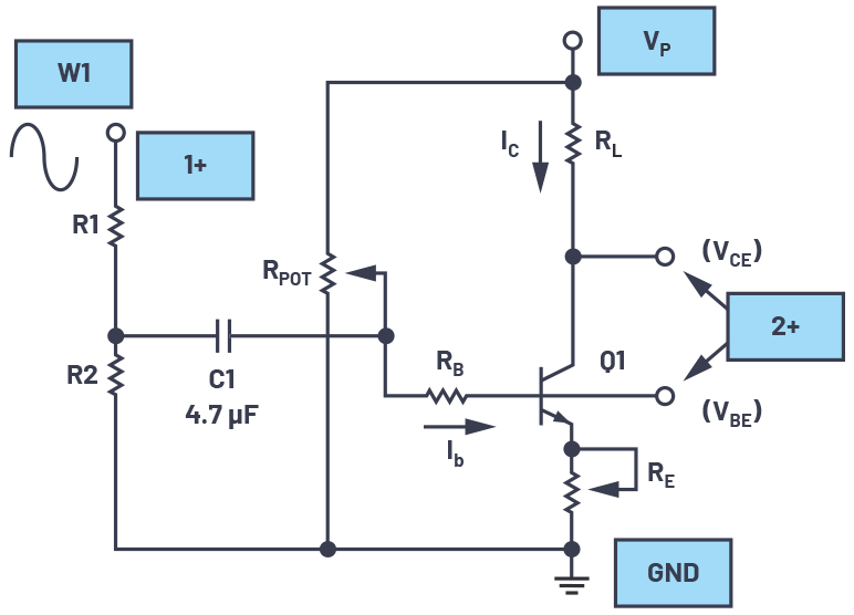
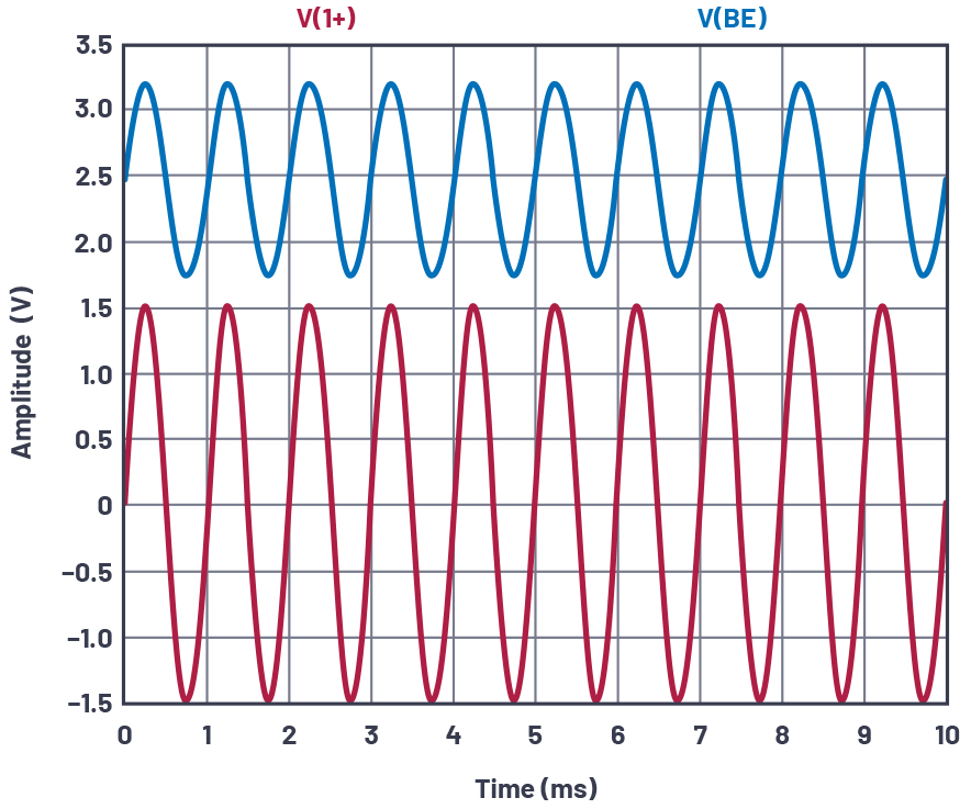
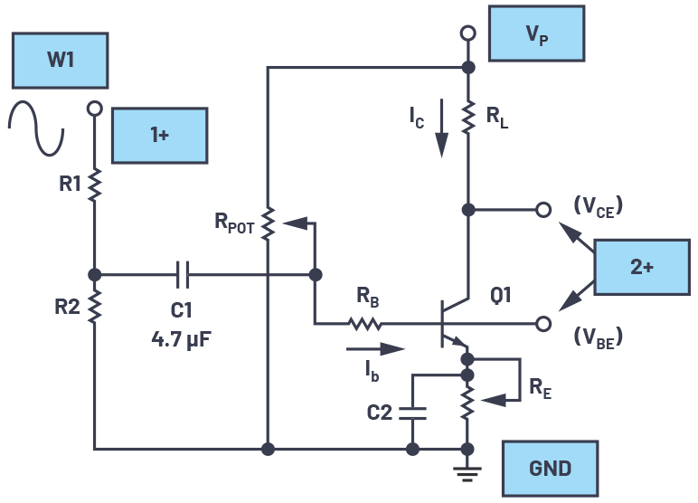
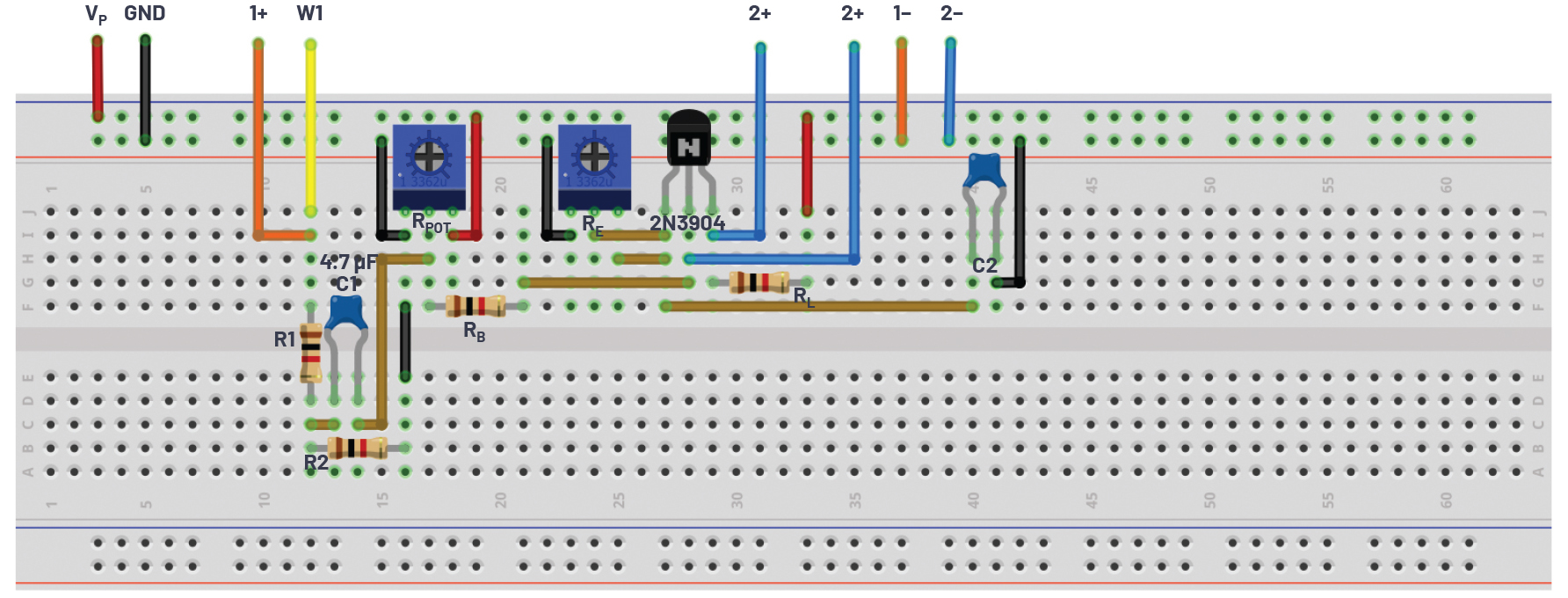
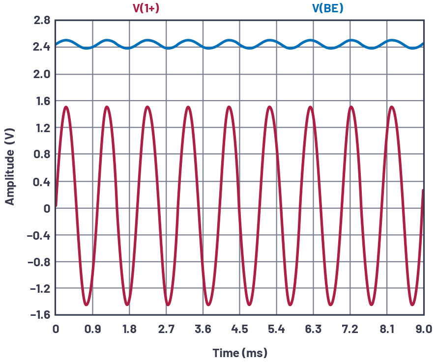
The configuration, shown in Figure 1, demonstrates the NPN transistor used as the common emitter amplifier. Output load resistor RL is chosen such that for the desired nominal collector current, IC, approximately one-half of the VP (5V) voltage appears at VCE. Adjustable resistor RPOT, along with RB, sets the nominal bias operating point for the transistor (IB) to set the required IC. Voltage divider R1/R2 is chosen to provide a sufficiently large attenuation of the input stimulus from waveform generator W1. This is done to more easily view the generator W1 signal, given the rather small signal that will appear at the base of the transistor, VBE. The attenuated waveform generator W1 signal is AC-coupled into the base of the transistor by the 4.7µF capacitor so as not to disturb the DC bias condition.
Hardware setup
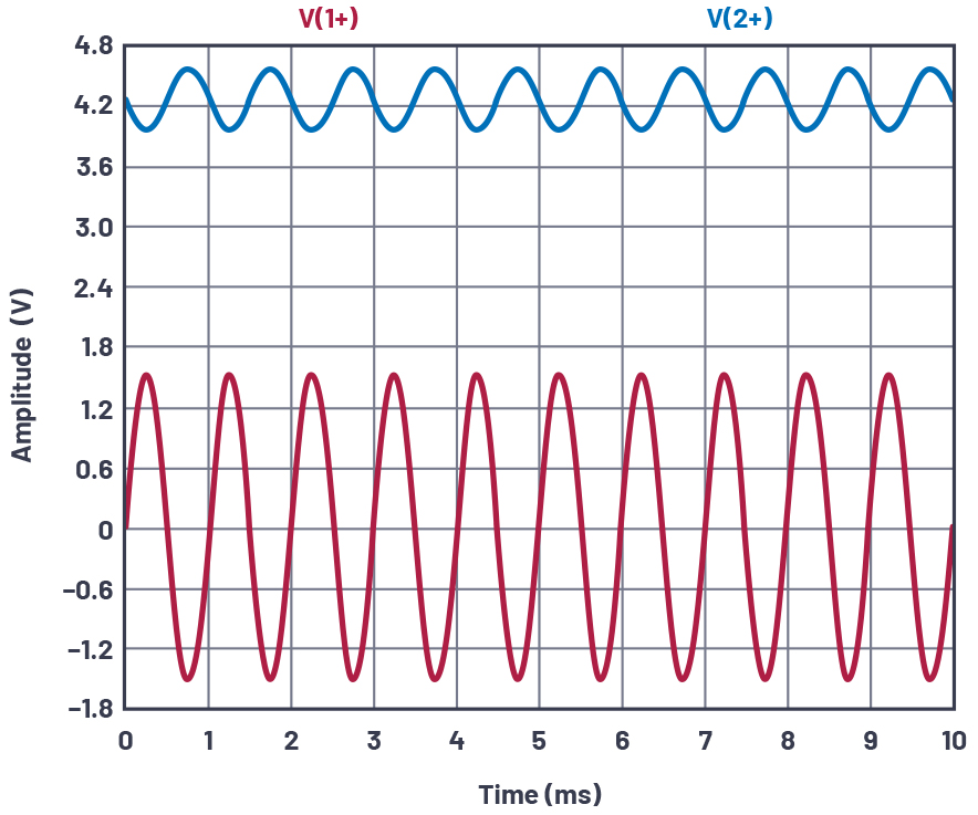
The waveform generator output W1 should be configured for a 1kHz sine wave with 3V amplitude peak-to-peak and 0V offset. The setup should be configured with Scope Channel 1+ connected to display the output W1. Scope Channel 2 (2+) is used to measure alternately the waveform at the base and collector of Q1.
Procedure
Turn on the power supplies connected to the collector (VP = 5V) of the BJT transistor.
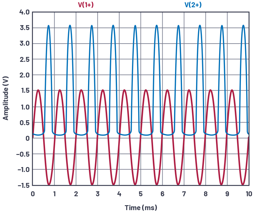
Configure the oscilloscope instrument to capture several periods of the input signal and the output signal.
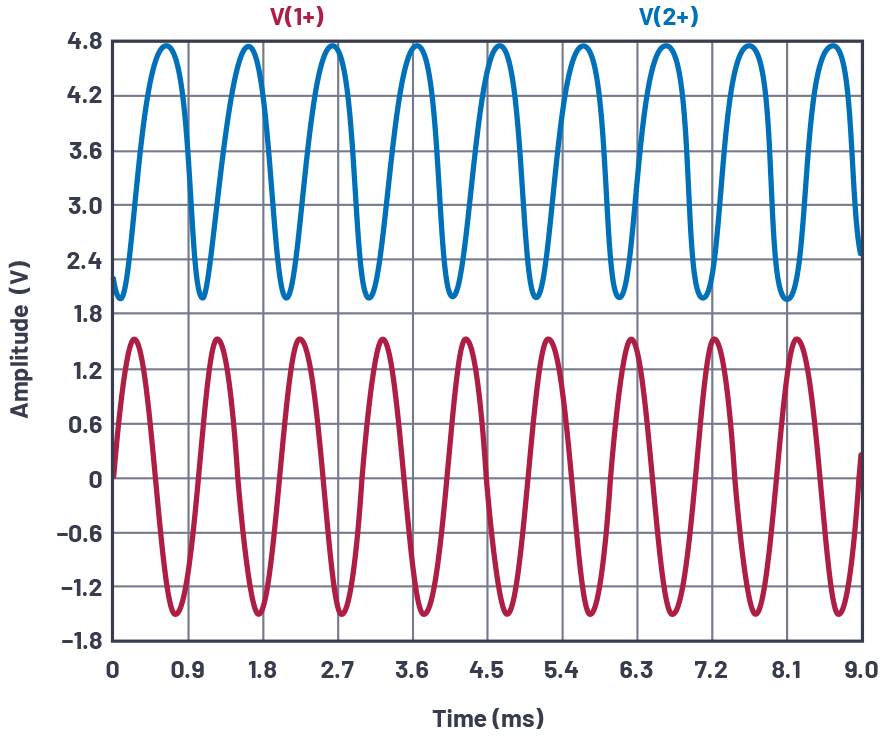
Plot examples of the simulated circuit using LTspice are presented in Figure 3 and Figure 4.

The voltage gain, A, of the common emitter amplifier can be expressed as the ratio of load resistor RL to the small signal emitter resistance, re. The transconductance, gm, of the transistor is a function of the collector current IC and the so-called thermal voltage, kT/q, which can be approximated by around 25mV or 26mV at room temperature.

The small signal emitter resistance is 1/gm and can be viewed as being in series with the emitter. Now with a signal applied to the base, the same current (neglecting base current) flows in re and the collector load RL. Thus, gain A is given by the ratio of RL to re.

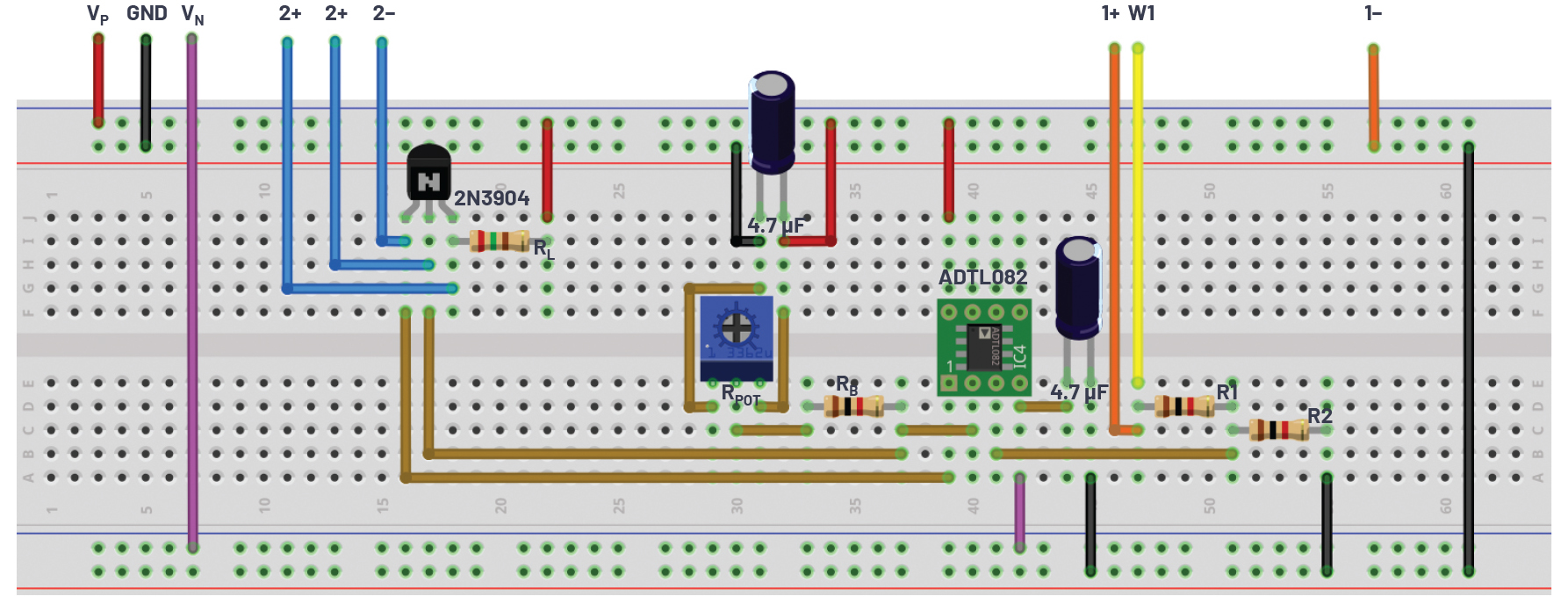
An alternative to produce a common emitter amplifier test circuit is shown in Figure 5. All the attributes are basically the same, with two slight advantages. One is that the base current bias is no longer dependent on the exponential base voltage (VBE). The second is that the summation of the small AC signal from the attenuated AWG 1 output is independent of the base bias circuit and does not need to be AC-coupled. The small signal AC input is applied to the non-inverting terminal of the operational amplifier (op amp), and thus, due to the negative feedback, also appears at the base of the transistor (inverting op amp input).

Self-biased configuration with negative feedback
Objective
The purpose of this section is to investigate the effect of adding negative feedback to stabilise the DC operating point. One of the most frequently used biasing circuits for a transistor circuit is the self-biasing of the emitter-bias circuit, where one or more biasing resistors are used to set up the initial DC values for the three transistor currents, IB, IC, and IE.
Hardware setup
The waveform generator output W1 should be configured for a 1kHz sine wave with 3V amplitude peak-to-peak and 0V offset. The setup should be configured with Scope Channel 1+ connected to display the output W1. Scope Channel 2 (2+) is used to alternately measure the waveform at the base and collector of Q1.

Procedure
Turn on the power supplies connected to the collector (VP = 5V) of the BJT transistor.
Configure the oscilloscope instrument to capture several periods of the input signal and the output signal.
Plot examples of the simulated circuit (using LTspice) are presented in Figure 11 and Figure 12.
Background
Common emitter amplifiers give the amplifier an inverted output and can have a very high gain, and can vary widely from one transistor to another. Additionally, the gain is somehow unpredictable due to temperature and bias current dependence. By introducing a small value feedback resistor in the amplifier stage, the performance of the circuit can be improved.
Additional materials
One 5kΩ variable resistor, potentiometer
Directions
Disconnect the emitter of Q1 from ground and insert RE, a 5kΩ potentiometer, as shown in Figure 13. Adjust RE while noting the output signal seen at the collector of the transistor.
Adding emitter degeneration
Objective
The purpose of this activity is to investigate the effect of the addition of emitter degeneration.
Hardware setup
The waveform generator output W1 should be configured for a 1kHz sine wave with 3V amplitude peak-to-peak and 0V offset. The setup should be configured with Scope Channel 1+ connected to display output W1. Scope Channel 2 (2+) is used to alternately measure the waveform at the base and collector of Q1.
Procedure
Turn on the power supplies connected to the collector (VP = 5V) of the BJT transistor.
Configure the oscilloscope instrument to capture several periods of the input signal and the output signal.
Plot examples of the simulated circuit (using LTspice) are presented in Figure 15 and Figure 16.
Increasing AC gain of an emitter degenerated amplifier
Adding the emitter degeneration resistor has improved the stability of the DC operating point at the lower cost amplifier gain. A higher gain for AC signals can be restored to some extent by adding capacitor C2 across the degeneration resistor RE, as shown in Figure 17.
Hardware setup
The waveform generator output W1 should be configured for a 1kHz sine wave with 3V amplitude peak-to-peak and 0V offset. The setup should be configured with Scope Channel 1+ connected to display the output W1. Scope Channel 2 (2+) is used to alternately measure the waveform at the base and collector of Q1.
Procedure
Turn on the power supplies connected to the collector (VP = 5V) of the BJT transistor.
Configure the oscilloscope instrument to capture several periods of the input signal and the output signal.
Plot examples of the simulated circuit (using LTspice) are presented in Figure 19 and Figure 20.
Questions
For the common emitter amplifier circuit setup, what is the effect on the voltage gain, A, by increasing RL?
You can find the answers at the StudentZone blog.
By Doug Mercer, Consulting Fellow, and Antoniu Miclaus, System Applications Engineer, Analog Devices.