


Mirtec, the South Korea–based manufacturer of optical inspection equipment, will showcase its latest semiconductor inspection system at Semicon West 2025 in Phoenix next month, as competition intensifies in advanced chip packaging.
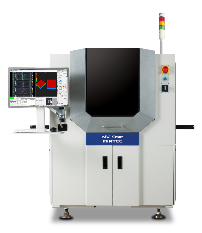
The company’s flagship product, the MV-9SIP Hybrid 3D Inspection System, will be on display at Booth 1955 during the three-day event. The system combines 3D digital blue moiré projection technology with a high-resolution blue laser scanner, enabling manufacturers to identify microscopic defects in tightly packed chip assemblies. Mirtec says its 25-megapixel CoaXPress vision system, developed in-house, offers higher precision in post-process semiconductor inspection than rival platforms.
Demand for inspection systems has risen as chipmakers adopt advanced packaging techniques such as system-in-package (SiP) and high-density solder bumping, both of which require more rigorous quality control. Mirtec’s technology is already being used beyond SiP inspection, extending to solder ball and bump analysis — processes that have grown more critical with the expansion of 5G, AI accelerators, and automotive electronics.
By combining multiple inspection methodologies into a single platform, Mirtec aims to differentiate itself in a market dominated by Japanese and US rivals. The company has also targeted high-reliability sectors such as aerospace and defence, where demand for defect-free semiconductor components is acute.
Semicon West 2025 will be held from the 7-9th October in Phoenix, Arizona.