


This article originally appeared in the April’23 magazine issue of Electronic Specifier Design – see ES’s Magazine Archives for more featured publications.
Jitter and power are analysed in both the time and frequency domains. Comparing PJ (periodic jitter) frequencies in the TIE spectrum to spurs in the power ripple spectrum is a fast and accurate way to identify signal integrity problems caused by the power distribution network (PDN). Jitter is measured relative to the system clock. Systems that use embedded clocking, where the clock is recovered from data transitions, mitigate low-frequency jitter but must be analysed with an oscilloscope capable of emulating the precise clock recovery scheme.
Signal integrity & power integrity contribute to errors
Digital errors are caused by jitter and noise. Noise is a broad term for variations in the signal amplitude. Jitter is the variation in the timing of bit transitions with respect to the data-rate clock, the so-called time interval error (TIE) and is caused by both phase noise and amplitude noise-to-jitter conversion. Noise-to-jitter conversion introduces problems from crosstalk, EMI (electromagnetic interference), and random noise.
Signal integrity analysis concentrates on the performance of the transmitter, reference clock, channel, and receiver in terms of the BER (bit error rate). Power integrity focuses on the PDN’s ability to provide constant voltage power rails and low impedance return paths. Signal integrity and power integrity have broad interdependence.
The PDN can cause noise and jitter. The circuit design and components – chip package, pins, traces, vias, connectors— affect the impedance of the PDN and hence the quality of the power supplied.
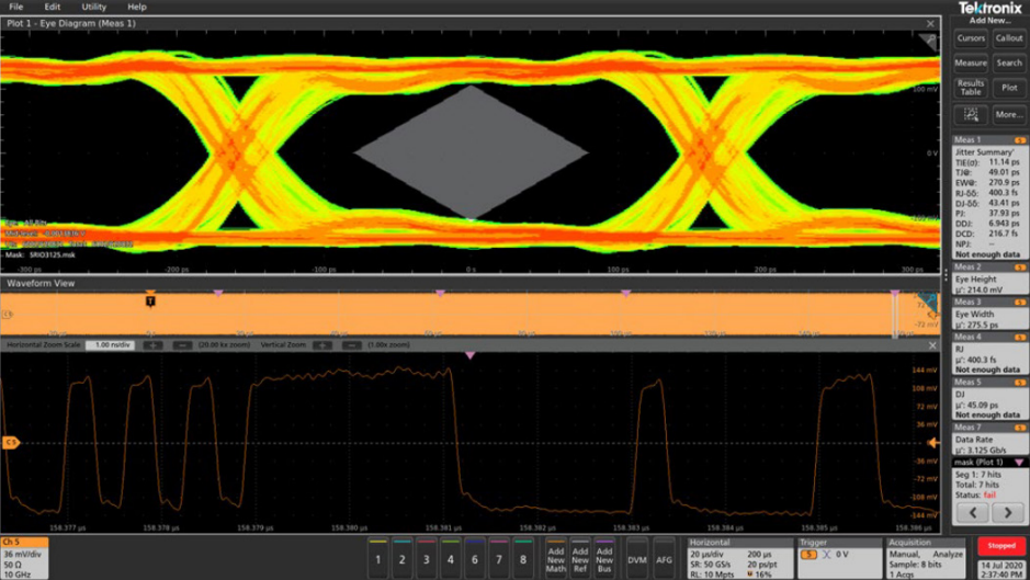
Figure 1. Eye diagram with mask test, top, and corresponding waveform, bottom.
Jitter and the power distribution network
The PDN’s job is to sustain a constant voltage and sufficient current supply to every active component. It impacts the performance of every element, active or passive. The PDN includes the whole system, not just the VRM (voltage-regulator module) and internal chip power distribution, but every interconnect, trace, via, connector, capacitor, package, pins, and ball-grids. Its performance depends on the SERDES properties and the effective series impedance of the system as a whole; ESR, ESC, and ESL (effective series resistance, capacitance, and inductance).
PJ & ground bounce
Power rail noise, often called ripple, is typically a few millivolts. Accurate measurements of mV noise on a power rail at GHz frequencies require high bandwidth probes with high DC impedance that act as 50 Ω transmission lines at high frequencies. Power rail probes are designed explicitly for this purpose. Power analysis can be automated on multiple power rails with the optional analysis packages which conveniently include key jitter measurements (TIE, RJ, DJ, PJ).
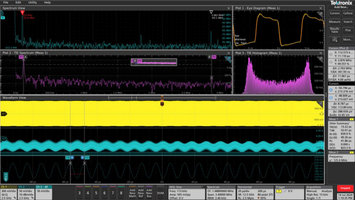
Figure 2. Power rail ripple in Spectrum View top left, and TIE spectrum just below it, along with the signal and power rail waveforms and the TIE histogram.
Switch-mode power supplies regulate the voltage between the power rail and the return path (a.k.a., ‘ground’) by continuously switching between low dissipation on and off states, achieving constant voltage by varying the on/off duty cycle. By avoiding high dissipation states, they waste much less power than linear supplies. Unfortunately, the pattern of on/off pulse widths that drive the switching elements can induce ‘switching noise’ and cause PJ.
Switching occurs at fixed frequencies that should be recorded on the VRM data sheet. If the ripple spectrum, top left of Figure 2, and the TIE spectrum, just below it, both have spurs at the switching frequencies, then we know the source and can address the design. Notice the large coinciding spur at the red marker in Figure 2. The TIE histogram to the right of the TIE spectrum has the signature sinusoidal jitter distribution (horseshoe), PJ at one frequency.
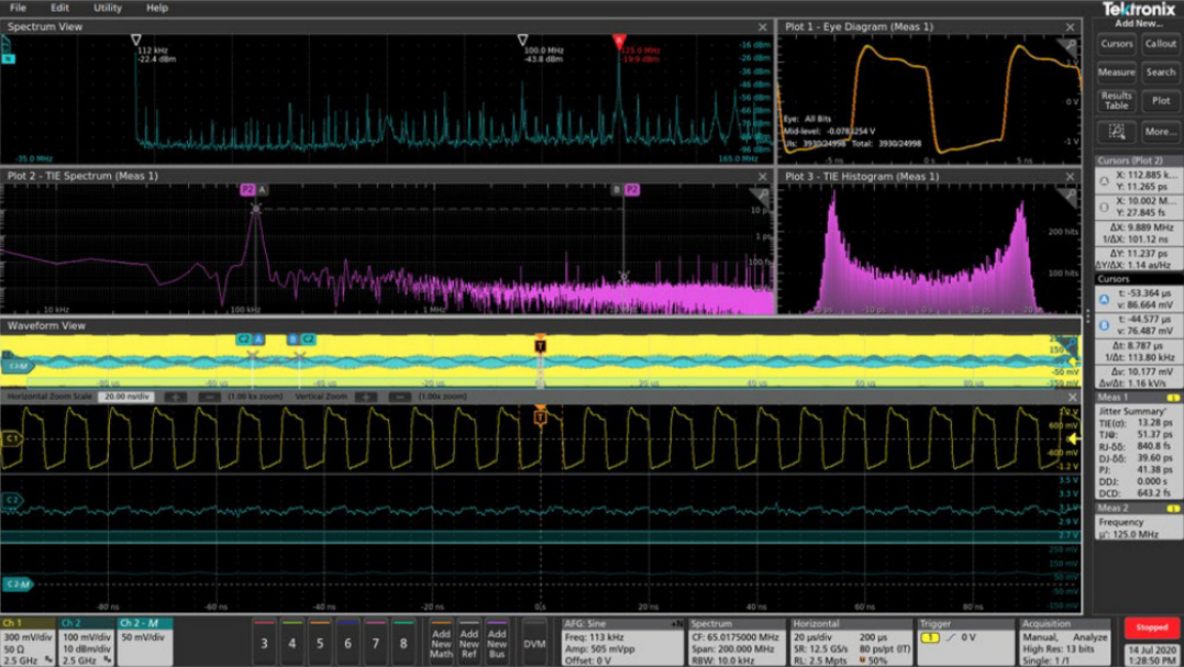
Figure 3. (a) Power rail ripple spectrum and (b) TIE/jitter spectrum
Introduction of charge density
Power supplies can introduce random noise that contributes to RJ. The power rail random noise shows up in Figure 2 as the noise floor of the Spectrum View plot in the upper left. RJ is calculated from the noise floor of the TIE spectrum. In this example, the random noise due to power ripple is very low, and RJ is tiny, about 0.84 ps.
During logic transitions, transmitters and receivers source or sink current from the PDN. When multiple signals switch between levels simultaneously, they can deposit or remove a substantial charge from the power rail and/or ground plane. The short-term introduction of charge density alters the voltage of what should be common ground across the conductor. The resulting voltage variation is called ground bounce or, equivalently, simultaneous switching noise (SSN).
Before continuing, we should clarify a couple of things. First, by ‘ground’ we’re referring to the desired common reference voltage of the return path which is usually defined to be 0V. Second, “simultaneous” means that the component’s source or sink charge during the time interval when their rise/fall times overlap.
SSN looks random in the time domain but not in the frequency domain. Data signals are composed of many frequency components—the fundamental or Nyquist frequency and perhaps as many as two higher harmonics, plus the subharmonics from consecutive identical bits. Simultaneous switching can occur at any of these frequencies. Thus, SSN is periodic noise with many low amplitude spurs that can cause PJ.
To confirm that the PJ is caused by SSN, compare the power rail spectrum, top left of Figure 3, with the TIE spectrum, just below it. The high amplitude spur that appears at the same frequency in both spectrums indicates a large PJ contribution from SSN.
Summary
Signal integrity and power integrity are a feedback loop. Every element of the network, every trace, via, connector, pin, package, etc, affects the PDN impedance and the impedance of every channel, and every active component can alter the voltages of power rails and ground planes.
The eye diagram can tell us a lot about signal integrity, but it rarely helps us identify specific issues, combining jitter and power analysis isolates otherwise difficult problems.
Signal integrity and power integrity are often considered separate disciplines, but we’ve seen that finding problems associated with high jitter requires understanding both.
Lee Morgan – Senior EMEA Technical Marketing Manager
Lee Morgan is EMEA Senior Technical Marketing Manager responsible for Tektronix Time Domain Business Unit.
Lee specialises in the embedded, power, and automotive sectors. With more than 20 years’ experience in the Test & Measurement sector, covering a multitude of roles in the Mobile Telecommunication, Electronic & Power industry, Lee has extensive knowledge and deep insight with respect to how modern Test & Measurement solutions can aid engineers of today, create the products of tomorrow.
