

This article originally appeared in the Feb’23 magazine issue of Electronic Specifier Design – see ES’s Magazine Archives for more featured publications.
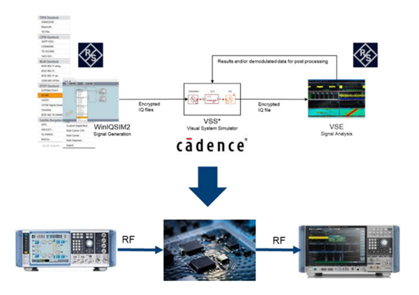
Figure 1. Software plugins bring high-quality signals and analysis tools into the EDA world.
In any engineering project, making the leap from simulation to hardware can be a potential disconnect in the path to product realisation. Will the design decisions informed by simulated results deliver the expected results in the real world? The complexity of modern radio standards like 5G and Wi-Fi make this an especially risky transition when designing an RF power amplifier (PA).
Making the leap
Designers of RF-amplifier ICs and systems both encounter a common frustration. In each case, development typically begins in an EDA environment and must inevitably move into the real world when the design is ready to commit to hardware. It’s a risky transition that can be difficult to judge. The step should be taken as soon as the simulated design is considered adequately proven. However, the accuracy of the results is often limited by the quality of the software signal sources and analysis tools available for use in the simulation environment.
Ideally, these signals should be representative of the appropriate wireless standard and measurements follow the standard’s procedures. However, the complexity of today’s cutting-edge wireless technologies like 5G and the latest Wi-Fi generations means this is not easily assured.
Wireless design challenges
Emerging radio standards present increasingly difficult challenges to engineers seeking to verify their designs. In addition to encompassing millimetre-wave (mmWave) frequencies, 5G standards often use complex massive multiple-in-multiple-out (MIMO) and beamforming topology that demands many coherent channels.
In the sub-6GHz frequency range (FR1), every path is typically connected to a digital back end, allowing individual linearization. Applications in the FR2 range can comprise antenna designs with up to 1024 elements, so hybrid beamforming is often used to converge subtiles to a single digital path.
On the other hand, higher bandwidths, up to 400MHz in one 5G FR2 carrier, are being used to increase data throughput, as well as higher-order modulation schemes that maximise utilisation of the occupied bandwidth. Similar developments can be seen in satellite space with digital regenerative payloads, basically a ‘base station in the sky’. Comparable enhancements are applied in electronic warfare for radar or other signals.
These, and other applications such as satellite communications that also use beamforming with phased-array antenna systems, call for a combination of highly linear and near-identical characteristics among large numbers of devices to ensure correct operation and maximise data throughput. Power-transistor technologies such as gallium nitride (GaN), used to cover the vastly increased bandwidth, introduce new challenges due to their inherent nonlinear behaviour. Higher order modulation schemes require smaller distortion levels as the distance between the constellation points becomes smaller. This imposes tougher limits for important parameters such as error vector magnitude (EVM) to ensure stable demodulation for maximised throughput.
To optimise efficiency of the RF frontend, the amplifier is operated close to its saturation point. This results in high nonlinearity, causing signal degradation, spurious signal generation, and – in digitally modulated signals – unwanted adjacent channel leakage ratio (ACLR). Newer PA technologies such as GaN offer greater efficiency and energy density but require linearisation in almost any use case.
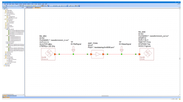
Figure 2. Software signal generator (left) and analyser (right) setup on VSS testbench.
Linking simulation and hardware worlds
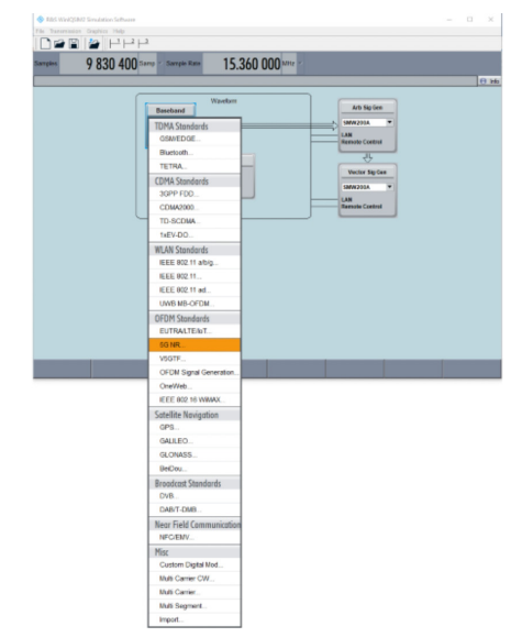
Figure 3. The simulation software R&S WinIQSIM2 supports a wide variety of wireless standards.
Committing a design to hardware, even after successful simulation, usually requires several iterations to achieve the desired real-world performance. Each iteration, however, adds cost and delays. The time to work out and implement the design revisions, approaching closer to the expected performance with each new version, can depend on the engineering resources assigned to the project: the number and skill level of available engineers and the tools available to complete the work.
Moreover, in the case of chip design, a contracted wafer fab may not be able to deliver the revised prototypes quickly for retesting. Late delivery of the new chips then puts the project behind schedule and can tie up resources and increase the risk of further delays. Moreover, the cost of each wafer run can easily reach six figures, adding further to the stress of the development process.
By avoiding these repeated hardware iterations, usually needed to meet the applicable performance for different radio standards, teams can control their development costs and stick to the intended schedule, ultimately aiming to be ready for market launch on time and on budget.
The performance of the chip or system, when simulated, can be verified by comparing important performance measurements with the specified system requirements. EVM, as a measure of signal linearity and a prerequisite for high data throughput, and other key performance indicators (KPIs) provide the information engineers need to understand whether the resulting system will deliver the expected performance when it is finally deployed.
When the KPIs suggested by simulation look good, the project can be considered ready to commit to hardware. From this point, measurements are taken using real-world signals. Standard-compliant waveforms are typically applied to systems such as 5G and Wi-Fi radios. On the other hand, equipment such as satellite communication devices typically use specially defined wideband digital modulation schemes.
Typically, the signals available in the EDA environment to drive the simulation may be more or less representative of those applied in the real world. In the absence of an exact correlation, ensuring that the hardware will perform as expected, so minimizing any need to redesign, re-simulate, remake, and re-test, calls for engineering judgement based on acquired experience of making this transition.
More recently, tools have emerged that can enable simulation based on properly stand[1]ards-compliant signals that are identical to those used in the real world. This removes the dependence on the engineer’s judgement: if the simulation results suggest the required performance has been met, the resulting chip may perform as expected in the real world.
Simulating the system in an EDA environment requires bringing standard signal generation and analysis software into simulation tools, where they can be implemented with the testbench containing the power amplifier as the DUT. There are various ways to achieve this. Rohde & Schwarz, for example, has collaborated with Cadence to create a software package, R&S VSESIM-VSS, that replicates state-of-the-art signal generation and analysis tools in the Cadence EDA tools (Figure 1).
Developing RF components and RF assemblies
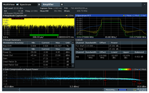
Figure 4. PA performance measurements including complementary cumulative distribution function (CCDF) and adjacent-channel leakage ratio (ACLR).
The package contains software equivalents with the signal generation software (R&S WinIQSIM2 simulation software) and vector signal explorer (R&SVSE) as plugins for Cadence Visual System Simulator (VSS) software. The VSS software environment for system simulation and modelling is part of the Cadence AWR Design Environment platform. It is particularly suited to developing RF components and RF assemblies used in wireless communications and radar design.
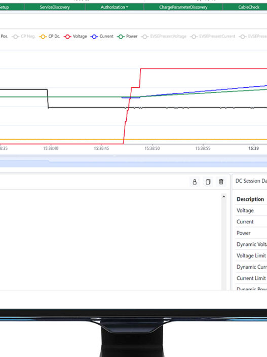
Working in the simulated test environment, the signal generator and signal analyser can be dropped onto the virtual testbench as data-source and data-sink function blocks connected to the DUT (Figure 2). In the simulation environment, the function blocks act as interfaces to the signal generation software and vector signal explorer, connecting the EDA and test and measurement software tools.
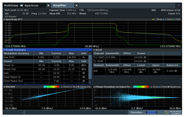
Figure 5. Measuring amplifier linearisation by applying Direct DPD.
R&S WinIQSIM2 generates standard-com[1]pliant signals (Figure 3). It supports all commonly used cellular and wireless connectivity standards, including 5G and Wi-Fi standards. In this way, realistic signal samples that are known to comply with the applicable wireless standard are incorporated in the simulator’s workflow to increase accuracy and simplify the design process. The signals are continuously maintained by the vendor and hence can be relied upon to be always up to date.
The vector signal explorer, R&S VSE, when connected to the output of the DUT, provides measurements for standard-compliant analysis.
In addition, the signal analysis software includes an RF PA test application that simplifies amplifier characterisation measurements such as compression, distortion, and EVM. The plugins can also be used in other tools of the Cadence EDA platform including Microwave Office circuit design software, which is used for monolithic microwave IC (MMIC) development and PCB-based amplifier design.
The data sink plug-in provides access to the signal at any point in the simulated design. The signal can be transferred to a vector signal generator and applied to available hardware, enabling system-level analysis of both hardware and simulated implementations.
Making realistic signals available within the simulation workflow permits an accurate prediction of the system performance and ultimately can help to reduce the number of hardware iterations needed to achieve the desired real-world performance.
The WinIQSIM2 simulation software and VSE functions for signal analysis use the same calculation methods as Rohde & Schwarz test instruments (figure 4). This simplifies the switch from software simulation to testing real hardware, maximising correlation between simulation and real-world RF testing by allowing test signals and demodulation setups to be reused. Ultimately, it enables a faster transition from the simulation running in the software environment to an implementation in hardware ready for the real world, greatly reducing risk and enabling the desired performance to be achieved after fewer design iterations.
However, designers of power amplifier ICs often also need to understand the PA performance when linearisation is applied to the output. PAs are typically operated in their non-linear region to deliver maximised RF output power with favourable efficiency. Optimal efficiency is desirable to minimise power consumption and circuit size due to cooling. Drawbacks of non-linear operation, on the other hand, include signal degradation and generation of spurious signals, or excessive adjacent-channel leakage ratio (ACLR) in the case of digitally modulated signals.
Simulating digital predistortion
Applying digital predistortion (DPD) is a commonly used technique to restore amplifier linearity. PA designers need to test their designs with DPD applied to predict the ultimate performance in terms of output power, efficiency, and linearity. The ability to predict the performance in this way is useful for amplifier IC designers, who need to understand when the design is ready to commit to final silicon, and for OEMs building amplifiers using such ICs to help optimise system performance.
Opportunities to simulate DPD in an EDA environment are usually very scarce. Developing a DPD algorithm is complex and typically carried out by specialist OEM teams. Rohde & Schwarz has developed a Direct DPD technique which bypasses algorithm development challenges by comparing the distorted amplifier output with an ideal reference to calculate the necessary distortion factor on a sample-by-sample basis. This Direct DPD technique can now be applied to PA simulations in Cadence EDA tools, including VSS and Microwave Office software.
By providing a convenient means of simulating PA performance with DPD, these connected tools enable chip designers to quickly assess their designs and thus reduce the number of wafer runs needed to achieve a result that will perform as required when delivered to customers. Knowing how the chip will perform when linearisation is applied helps ensure the IC will perform as the user expects and helps chip makers properly support their customers and the products.
Chip design teams tend not to have extensive signal-design expertise in-house, so creating suitable signal sources in software to help understand the amplifier’s linearisability is a challenge. RF-system OEMs, for their part, can do more of their design validation work within the EDA tools and so can alleviate a significant element of risk associated with moving from the software-based simulation environment to prototype hardware. It lets designers evaluate linearisability without in-depth knowledge of DPD techniques.
Moreover, Direct DPD can be applied to the hardware in the same way as in simulation (Figure 5). The techniques used to apply DPD in the EDA environment provides an early insight into linearisation benefits. Using the same approach in real hardware ensures consistency between the predictions gained from simulation and performance seen in the real world.
Conclusion
Today’s EDA tools have simplified and accelerated many complex challenges associated with designing RF ICs and systems to support advanced wireless standards. However, making the transition from the virtual solution that exists within the EDA environment to real hardware remains a significant risk.
Where there is a disconnect between the evaluation tools and signals used in the EDA environment and those used in the real world, there is a risk that the predicted performance will not be achieved at the first attempt. Any subsequent hardware iterations add significant cost and time to the project.
Eliminating that disconnect by taking advantage of closer collaboration between EDA and test equipment vendors can mitigate those risks. In particular, access to accurate, standards-compliant signal creation and analysis helps ensure the real-world performance mirrors closely the results predicted by simulation. The ability to apply digital pre-distortion within the EDA environment gives designers valuable extra power to create amplifiers that respond well to linearisation.