


“The SLC is designed to provide excellent clock or LO (local oscillator) substitution signals to semiconductors where jitter and noise really matter. Typically, the SLC will be used to drive data converters (ADC and DAC), direct digital synthesisers (DDS) or high-speed FPGAs and serial links to achieve the highest performance,” said Guillaume de Giovanni, President, Noise XT.
Most of the clock sources on the market today are either noisy digital boards or traditional signal generators—losing quality at useful frequencies. To discern the quality of a clock source, a typical figure is the amount of jitter, which is related to phase noise.
The SLC offers two clean clocks in a single compact package to achieve low jitter measurements down to -170dBc/Hz at 10MHz and 40fs (femtoseconds) RMS on a 155MHz clock for example.
Wireless applications, particle colliders, digital semiconductor testing, and network time synchronisation are a few of the many applications. Products that will benefit most from using the SLC are digital transceivers used in Software Defined Radio (SDR) applications and high-speed semiconductor testers. The SLC is used as either a local oscillator or as a clock in single or dual configurations allowing smaller footprint per channel.
In jitter measurements, the lower the jitter, the more accurate the time will be, enabling more bandwidth, and better signal-to-noise (SNR) ratio. The result is fewer transmission errors and better detection of weak signals.
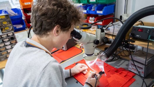
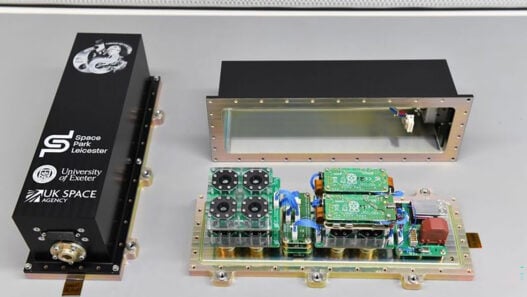
The SLC uses the latest component technology to maximise the cost/performance ratio on a 100 x 160 mm internal board. The unique combination of multi-DDS (Digital Direct Synthesis) with PLL (Phase-Locked Loop) is used to achieve the SLC’s ultra-low jitter performance.