Ivan Hoo, Senior Equity Campaign Manager at Crowdcube, commented: “Nanusens is one of the first electronic component manufacturers to use Crowdcube for fund raising. A business like this could have issues in translating the technical complexities to our investors but the management team at Nanusens have done an excellent job in communicating the intricacies of their business plan. As a result, the campaign has received tremendous support from retail investors as well as sophisticated investors.”
The problem that Nanusens solves is that the demand for sensors is exceeding the current production capabilities. This is a problem that is getting worse as more and more devices are being designed with a range of sensors to provide awareness and make them smart, with smartphones being one of the leading examples that has helped the sensor market grow to billions of units a year.
The bottleneck is caused by current production methods requiring specialist techniques that makes it hard to ramp up production. Nanusens has developed a way to use the same standard techniques used in the giant production facilities that make most of the world’s electronic chips.
This means that there is no limit to the number of sensor chips that Nanusens can make as they can be made in any of these facilities. Nanusens predicts that it could increase the size of the sensor market from billions of units to trillions of units by solving this production bottleneck.
“The Internet of Things has been forecast to need trillions of sensors,” explained Dr Josep Montanyà, Nanusens CEO: “but current sensor production methods cannot support such numbers. We will be able to and at the right price for the market. This will finally enable the IoT to grow as predicted.”
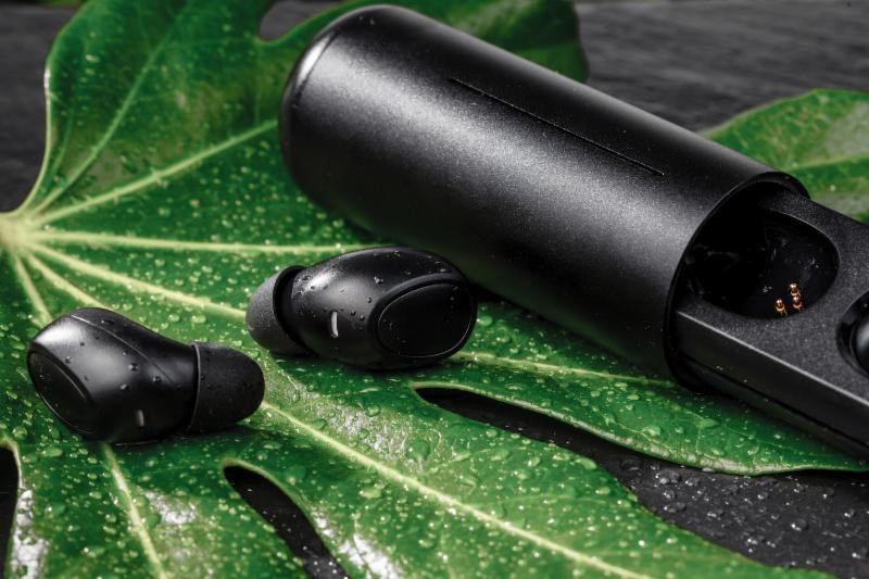
The first target market on this journey is earbuds. These need a number of ultra-small sensors to provide an enhanced user experience. Nanusens’ breakthrough technology enables it to make sensors that are less than a quarter of the size of current designs. This frees up space inside the earbud design for larger batteries for a longer operational life or more sensors for additional features.

Simon Forrest, Principal Technology Analyst, Futuresource Consulting, said in the 2019 Futuresource Hearables Market Report – Worldwide: “Space is always at a premium within hearables; similarly so is battery life. Adding more sensors to create ‘smart’ hearable products is therefore challenging. The answer may come from advances in MEMS manufacturing. European start-up, Nanusens, have developed methods to create MEMS sensors within standardised CMOS manufacturing processes. This enables sensors to be placed on the same silicon as the control logic, making them up to ten times smaller and freeing space for other components or larger batteries.”

Technical infomation
These sensors are called MEMS (Micro Electro Mechanical Systems) that have tiny moving parts and each design of sensor requires a custom production line. Thus, the only way to increase production of a particular MEMS sensor type is to build a duplicate production line. This means that production is very hard to ramp up creating a bottleneck with demand exceeding supply and getting worse as more devices are designed with sensors in them.
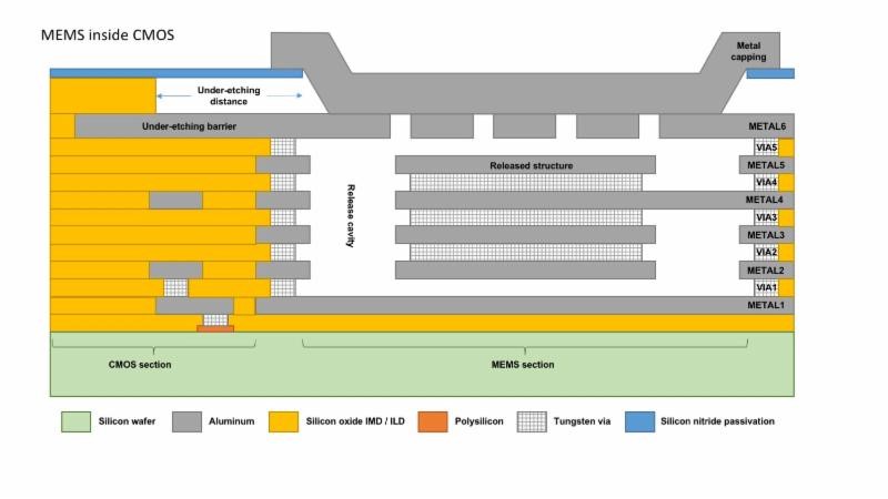
Nanusens solves this by making MEMS sensors with the same standard production processes, called CMOS, that are used to make electronic chips in huge numbers in the giant production facilities, called fabs, around the world. Its unique approach builds the metal sensor structures within the chip rather than on the surface as is done currently. This means that Nanusens can have its sensor chips made in any fab, in whatever volumes it requires, solving the volume production barrier of current MEMS products. This unlocks the MEMS market so that it can now grow to the trillions as has been predicted but so far has been unable to realise.
In theory, this sounds very simple to do. In practice, it is very hard because the CMOS process was never designed for this purpose. The released metal structures have stresses and so distort rendering them useless. Nanusens has spent years researching and perfecting structure designs that do not distort when released. These, and variations thereof, are being patented to prevent others trying to copy Nanusens technology of NEMS-within-CMOS to create nanosensors.


