


When Power Integrations announced new members of its InnoSwitch 3 families of offline CV/CC flyback switcher ICs, the company reported that the new ICs feature up to 95% efficiency across the full load range and up to 100W in enclosed adapter implementations without requiring a heatsink. This increase in performance was achieved using an internally developed high-voltage Gallium Nitride (GaN) switch technology (PowiGaN).
The InnoSwitch3, InnoSwitch3-Pro and LYTSwitchTM-6 families of flyback power conversion ICs (Figure 1) eliminate the need for heatsinks in chargers, adapters, LED ballasts and other compact or sealed power systems with negligible airflow. InnoSwitch devices utilise the company’s FluxLinkM feedback system and provide high regulation accuracy, rapid transient response and a comprehensive suite of line, load and self- protection features. The InnoSwitch3 is suitable for USB-PD and programmable power supply (PPS) rapid charging adapters, consumer product, appliance and industrial applications when high efficiency, high reliability and survivability, low component count and compact layout are critical to design success.

Figure 1: InSOP-24C proprietary surface mount power package used by the InnoSwitch3, InnoSwitch3-Pro and LYTSwitch-6 families
The low-profile InSOP-24C package used for these devices is able to deliver between 30 and 60W without a heatsink, depending on the input voltage range and power supply form factor using proprietary silicon MOSFET technology.
To deliver the power needed for higher power rapid charging, IoT-connected appliances, LED lighting and industrial applications and to further reduce converter size, a primary power switch with lower RDS(ON) per unit area and higher conversion efficiency is required. Wide band-gap semiconductors provide lower specific RDS(ON) (on resistance per unit area) and greatly reduced switching losses.
GaN switch technology
GaN is a wide bandgap semiconductor material that allows the fabrication of switches that have very low switching losses both during turn-on and turn-off compared to their silicon counter parts. Unlike silicon MOSFETs, GaN switches inherently have near-zero turn-off losses. Turn-on losses in GaN switches are almost entirely due to inter nodal capacitances which are much smaller in GaN compared to silicon MOSFETs. This is because both turn-on and turn-off in GaN are almost instantaneous and equivalent RDS(ON) GaN devices are much smaller in die size than silicon (see Figure 2).
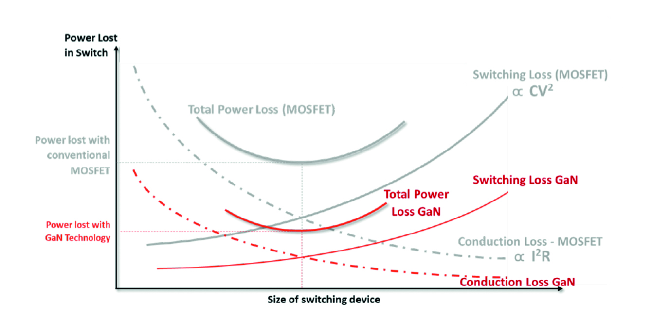
Figure 2: Comparison of the conduction losses (channel resistance) with switching losses in a GaN device and a silicon device
PowiGaN devices are optimized for use in the company’s integrated power solutions. They allow the InSOP-24C package to deliver much higher power levels without a heatsink while also substantially increasing the overall power supply efficiency, says the company.
A major challenge for discrete GaN solutions is the difficulty in driving the transistors and protecting them. GaN is much faster than silicon to the degree that even small amounts of inductance and capacitance introduced by the discrete GaN packages and PCB trace connections makes it very difficult to drive. Common challenges faced by designers are high a dv/dt and high frequency oscillation during switching which creates EMI, lowers efficiency and some cases can cause destruction of the device. The high switching speed also makes it very difficult to protect the transistor during fault conditions as the high speed of the GaN switches can cause the switch current to ramp to destructive levels – before the protection circuitry has a chance to safely turn off the device.
Embedding the PowiGaN in the company’s integrated switcher ICs significantly reduces parasitic inductances and capacitances making it easier to avoid oscillation. PowiGaN-based products incorporate drivers that are tailored to the specific PowiGaN device, optimising switching speed to minimise EMI, maximise efficiency and to effectively eliminate oscillation, the company reports. The protection circuitry is able to quickly detect unsafe currents to safely shut down a device under fault conditions. The switching converter ICs include start-up circuitry which eliminates the need for external biasing circuits.
PowiGaN devices also employ lossless current-sense technology, eliminating external sense resistors that frequently exceed the resistance of the GaN switch itself in discrete implementations. As a result, the company says that power supply developers can focus on meeting customer’s power delivery, form factor and thermal requirements, without worry about the needs of the enabling GaN technology.
Software support
The operation of PowiGaN-based InnoSwitch3 is indistinguishable from that of conventional (silicon- based) devices from the same family. Switching frequency, transformer design, EMI filtering, biasing and synchronous rectification circuitry is identical for PowiGaN and silicon devices. Changes are only necessary to accommodate the higher power of PowiGaN-based designs. The PI Expert automated power supply design software suite supports both MOSFET and PowiGaN-based devices. This speeds up the design process by enabling the selecting of the best component and generating the full schematic, magnetics and BoM from basic parametric inputs.
The seamless transition between GaN and Silicon devices is demonstrated by the comparison of drain-source voltage waveforms during switching for PowiGaN and silicon InnoSwitch3 devices. This is shown in Figure 3, note that the waveforms are virtually identical; the same circuits can be used for silicon and PowiGaN-based devices. The faster turn-on characteristic of the PowiGaN switches can be seen in Figure 3(c); however the slope of the transition is the same and produces a similar EMI signature.
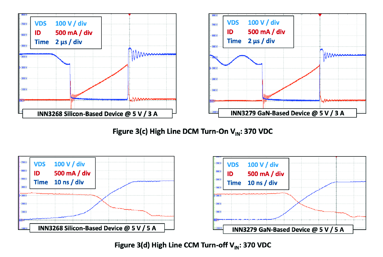
Figure 3: The drain-source voltage waveforms demonstrate seamless transition between GaN and silicon devices
Efficiency for PowiGaN-based designs is constant across line and load ranges. This makes them particularly suitable for applications calling for high average efficiency and for adjustable output voltage designs (e.g. USB PD and PPS).
The high full load efficiency across line voltage enables InnoSwitch3 designs to eliminate heatsinks for the smallest possible converter size. An example of this is shown in Figure 4.
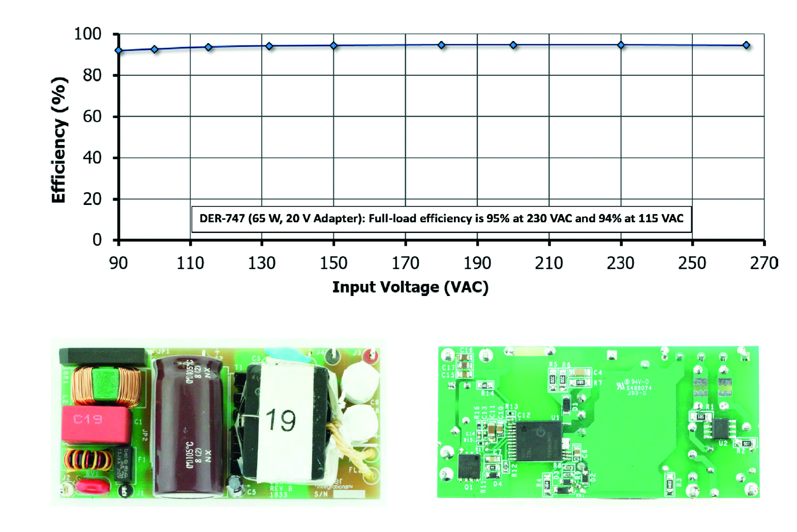
Figure 4: The DER-747 is a 65W adapter using InnoSwitch3-EP INN3679C
In USB PD type applications, the need to accommodate multiple output voltage options limits transformer optimisation and reduces efficiency. The company reports that InnoSwitch3 devices using PowiGaN switches still achieve high efficiency across load and are able to eliminate the heatsink for rapid- charge designs.
Real-world testing
PowiGaN devices are specifically designed to operate at the voltage levels seen in off-line flyback power conversion. They are manufactured in the same fabs as the company’s conventional silicon products and have undergone extensive qualification testing to ensure reliable operation in power conversion circuits. The qualification tests include pre-conditioning and moisture sensitivity level (MSL), temperature humidity bias, temperature cycling, high temperature storage life, dynamic operating life, highly accelerated life test, high temperature reverse bias, pre-conditioning, MSL, temperature humidity bias, temperature cycling and high temperature storage life. The switcher ICs also go through extensive long-term testing in real-world power supply designs which has resulted in a field failure rate of less than 0.2 parts per million (PPM).
In addition to the standard qualification tests employed, PowiGaN-based product qualification includes additional DOPL and HALT testing to confirm an extra degree of survivability for these devices in worst case (real-world) conditions (Figure 7). As part of the PowiGaN development process, unique and proprietary wafer level, die level and final-test level GaN-specific screening tests have been created to ensure device continuity and reliability.
Voltage considerations
The company’s switcher devices operate at the highly variable range of mains voltage levels encountered in the off-line power conversion applications worldwide. Voltage stress on the primary switch in a flyback power supply is a combination of the rectified line voltage (VBUS) the output reflected voltage (VOR) – the output voltage reflected across the turns-ratio of the power transformer and the voltage induced by the leakage inductance of the transformer primary winding (VLE). In a typical flyback design the worst case voltage stress under normal operation occurs at maximum line voltage (264V AC for European systems).
All InnoSwitch3 families and LYTSwitch-6 devices monitor bus voltage via the V pin and will interrupt switching to eliminate VOR and VLE voltage-stress components during line surges.
Power supplies attached to mains may also experience line surges and swells. Two voltage ratings for the PowiGaN switch enable the engineer to optimise the power supply design for practical applications. The VMAX(non repetitive) rating (750V) describes the maximum voltage-withstand under transient, swell and surge conditions. PowiGaN- based parts are 100% production tested at voltages in excess of this limit to ensure operational reliability. This parameter is employed for derating purposes in the power supply design in the same way as the absolute max BVDss rating for a traditional MOSFET is used. The maximum continuous voltage parameter describes the stress that may be applied continuously to the GaN switch. For PowiGaN devices this figure is 650V. Operation above this limit will not damage the device, but repeated exposure to higher voltages may cause temporary RDS(ON) shift beyond the limits described in the datasheet.
InnoSwitch products are provided with a fast line-over-voltage protection feature. This means they will cease switching to protect themselves in the event that the line voltage exceeds a user-defined limit. In this way, the design ensure that all of the 750V of maximum voltage rating is available during transients.
As a material for power semiconductors, GaN enables devices that behave much closer to an “ideal switch” than contemporary silicon. The technology used in the PowiGaN-based InnoSwitch3, InnoSwitch3-Pro and LYTSwitch-6 is effective, reliable and easy to use, says the company, and the performance of PowiGaN-based devices means that the technology will be increasingly used in its future device families.