


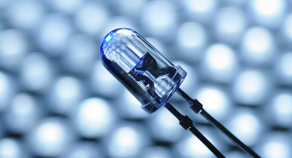
High power LEDs (HP LEDs) are rapidly becoming normal for demanding applications and are starting to make forays into more conventional applications such as the domestic and commercial settings. There is, however, a problem.
Only around 30% of the power put into LEDs is converted into visible light; the remainder is converted into heat. As the current increases the LEDs run hotter, and this puts the integrity of the LED at risk. Lifespan, colour rendering and reliability are all adversely affected by too much heat.
This heat needs to be removed as quickly as possible. The question is how to achieve this at a price that makes commercial sense. According to the US Department of Energy (DOE) if LEDs are to become truly ubiquitous they need to be cheaper. Adding cost by using expensive thermal management options would be seriously counter-productive.
If LEDs can be kept cool enough, it is possible to use fewer of them to generate the same brightness. The DOE estimates the LEDs and optics in a downlighter make up around 55% of the bill of materials cost, so reducing the number of LEDs in a device can slash the cost.
To generate the same lumen output with fewer LEDs, however, requires driving the remaining LEDs much harder. This significantly increases the heat of the LEDs – heat that needs removing quickly before it compromises the integrity of the LED. Thermal management now becomes a commercial as well as a technical imperative.
Existing approaches – and problems
There are three ways to remove heat – convection, conduction and radiation. As most LEDs are encapsulated in a transparent resin (a very poor thermal conductor) this limits convection and radiation in most designs. Heat is conducted through the back of the chip, to the PCB, through the heatsink and into the atmosphere. The smaller the thermal resistance along this path, the quicker the heat will dissipate.
Most HP LEDs are mounted onto a thermally conductive PCB to minimise the thermal resistance between junction and heatsink rather than on traditional resin based FR4 boards. The PCB spreads the heat from the LED junction across the board and through into the heat sink, cooling the LED. There are two varieties of thermally conductive PCBs: metal or ceramic.
Ceramics such as aluminium nitride (AIN) offer excellent thermal conduction and also provide electrical insulation and act as a thermally conductive dielectric. There are drawbacks: AIN is expensive and brittle. In contrast, alumina (Al2O3) is common and more cost-effective – but has significantly lower performance, while still being brittle and limited to very small board sizes. For this reason, ceramic PCBs tend to be found in very high-end applications or within the LED package itself.
Metal Clad PCBs (MCPCBs) are the most commonly used substrate for HP LEDs. They are typically made from cost-effective aluminium which is robust, lightweight and an excellent thermal conductor. It is also a conductor of electricity and this presents a problem, namely how to make aluminium into a thermally conductive dielectric.
A huge effort has been undertaken to develop effective thermally conductive dielectric layers. Typically these are epoxy resins filled with ceramics; but this approach has limitations. Increasing the ceramic content in the resin can affect the adhesion of the dielectric to the aluminium, compromising the long-term reliability of the PCB. These epoxies are affected by temperature cycling and can crack.
A new approach to thermal management
A process has been developed by Cambridge Nanotherm to convert the surface of aluminium to ceramic. This uniform ceramic layer, a nano-ceramic, acts as a “perfect” dielectric, says the company.
The layer can be built between three to 30µm in thickness. The size of crystallites is tiny – approximately 40µm. This size plays a critical role in giving the layer high thermal conductivity (7.2W/mk), high dielectric strength (around 50 /µm) and flexibility (clearly visible when the nano-ceramic is applied on foil substrates). The thickness of the dielectric layer can be tightly controlled to provide a close match to a product’s breakdown voltage requirements.
Board layout
To complete the PCB, a copper circuit is laid onto the ceramic layer. This involves laminating copper foil and using thin-film techniques to create a metal seed layer with further galvanic copperbuild.
Thin film is thermally efficient, while copperlamination to the dielectric surface offers a more cost-effective option and high-performance bonding system. In the case of nano-ceramic MCPCBs the thermal resistance of typically 1.5mm aluminium boards using the thin-film technique is low at 0.101⁰C.cm²/W (rivalling the performance of aluminium nitride ceramic). For the same aluminium thickness, laminated copper with 10µm ceramic provides 0.302⁰C.cm2/W, which is 20 to 30% better than any other aluminium MCPCB, beating even the highest performance copper MCPCBs.
The thermal demands of HP LEDs climb meaning more high-power applications are beyond the thermal capabilities of FR4 or resin-coated MCPCBs. This leaves designers with a simple choice: expensive, difficult to work with ceramics or cost-effective, robust nano-ceramics.