


The bus cables of industrial RS-485 networks typically share the same conduits with industrial DC supply buses. Short circuits can occur between the data and supply conductors due to cable mis-wiring and insulation breaks caused by sharp cable bends. To survive these fault conditions, over-voltage protected transceivers are needed. Their bus terminals possess high DC and AC stand-off voltages that exceed the maximum possible DC supply voltage.
However, protecting bus data lines against even higher over-voltage transients, such as lightning strikes, requires transient voltage suppressors (TVS) with specific switching characteristics.
A transceiver like the one in Figure 1 can withstand AC and DC over voltages of up to ±60V. One bus line can hang at +60V while the other bus line sits at -60V. This results in an impressive differential of 120V. Transient events according to EIA-485 can even reach up to ±80V.
Withstanding such high voltages is easy for a disabled transceiver, which simply relies on the high breakdown voltages of its output transistors. However, over voltages often occur during the most inconvenient times, such as data transmissions. In this case, one of the bus drivers is enabled, trying to pump enough current down the line for the remote located receivers to detect.
Current limiting
To prevent serious damage to the driver, a clever current limiting scheme is needed to enable the driver to transmit data whenever possible and limit its current during a fault event. Fault-protected transceivers have driver stages with double fold-back current limiting that typically provide a common-mode range much wider than specified in the RS-485 standard.
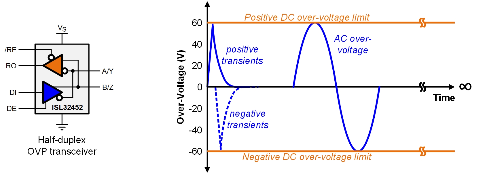 Figure 1: Over-voltage protected RS-485 transceiver Symbol and voltage range.
Figure 2 shows the current limiting function of the fault-protected transceiver in Figure 1. It operates over the wide common mode range of ±20V. The first fold-back current level of about 63mA ensures that the driver never folds back when driving loads within the entire 40V (±20V) common mode range. A lower second fold-back current level (~13mA) minimises power dissipation during an over-voltage fault event. This current limiting scheme ensures that the driver output current never exceeds the RS-485 specification, even at the common-mode and over-voltage range extremes.
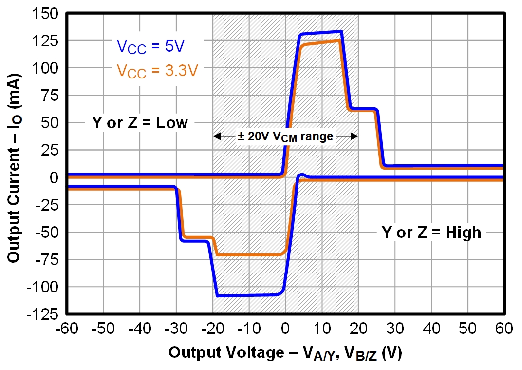 Figure 2: Double fold-back current limiting.
In the event of a major short-circuit condition, the transceiver also provides a thermal shutdown function that disables the driver whenever the die temperature becomes excessive. This reduces power dissipation to zero and allows the die to cool. The driver automatically re-enables after the die temperature drops by about 15°C. If the fault condition persists, the thermal shutdown/re-enable cycle repeats until the fault is cleared. The receiver remains operational during thermal shutdown, and fault-protection is active regardless of whether the driver is enabled, disabled, or the IC is powered down.
Internal ESD protection
The transceiver internal ESD protection is accomplished with silicon-controlled rectifiers (SCRs). These devices have a snapback rather than a Zener characteristic. They start conducting when an external voltage exceeds their trigger voltage threshold. Because of the driver output transistors’ high breakdown voltage, the trigger threshold is ±70V to prevent erroneous triggering during normal operation. The transceiver’s symmetrical snapback characteristic is shown in blue in Figure 3.
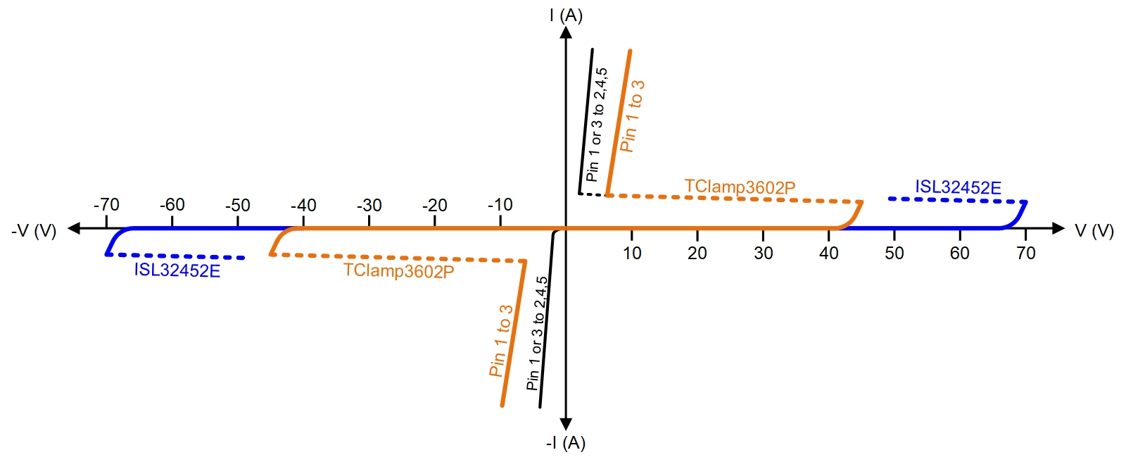 Figure 3: Snapback characteristics of transceiver ESD cells and external TVS diode.
Setting the trigger thresholds far outside the operation limits provides the benefit of using a wide range of TVS devices, whose high clamping voltages remain below the trigger thresholds.
Many TVS devices protect against the three major types of over-voltage transients: electrostatic dischard (ESD), electrical fast transient (EFT), and surge. To survive DC potentials of up to 36V, a TVS must have a working voltage of similar value and a reverse breakdown voltage of more than 40V (the working voltage’s leakage current into the TVS stays below 1mA). This is followed by the reverse breakdown, where the device starts slightly conducting and the current increases to 10mA.
Despite its high breakdown voltage, accompanied by a 350mW power absorption capability, this TVS has a footprint of only 2.0 x 1.0mm. Terminals 1 and 3 connect to the data lines while terminals two, four and five are the ground connection.
There are two wiring options. Using one TVS to protect two data lines leads to an asymmetrical clamping profile. Applying test pulses with positive polarity to the A and B conductors causes the transient currents to flow through a steering diode and the centre snapback device. For negative pulses, the currents only pass through a single diode. Figure 3 shows the asymmetrical clamping characteristics in black lines, denoted as Pin 1 or 3 to 2, 4, 5.
Using two TVS devices, one for each data line, results in the symmetrical clamping characteristic, denoted in Figure 3 as Pin 1 to 3. Here the ground pins 2, 4, and 5 are not connected. Instead one of the I/O terminals, 1 or 3, connect to a data line and the other one to ground. Thus, the flow of transient current for positive and negative pulses remains symmetrical.
As shown in Figure 3, the trigger thresholds of the TVS devices are below the trigger thresholds of the transceiver’s internal silicon controlled rectifiers (SCRs), thus preventing interaction between the internal and external protection schemes.
Final circuit design
The asymmetrical clamping of the single TVS solution drastically limits the transceiver’s common mode range for negative common mode voltages. This should only be used in applications with small common mode variations. Otherwise, each line must be protected with a single TVS. The added footprint of 2mm2 makes full use of ±20V common mode range and ensures RS-485 compliance is achieved. Another benefit to using a TVS is its low junction capacitance of 4pF (max). This allows the designer to either protect each single node in long-haul networks or protect high-speed (40Mbps) point-to-point data links without affecting signal integrity.
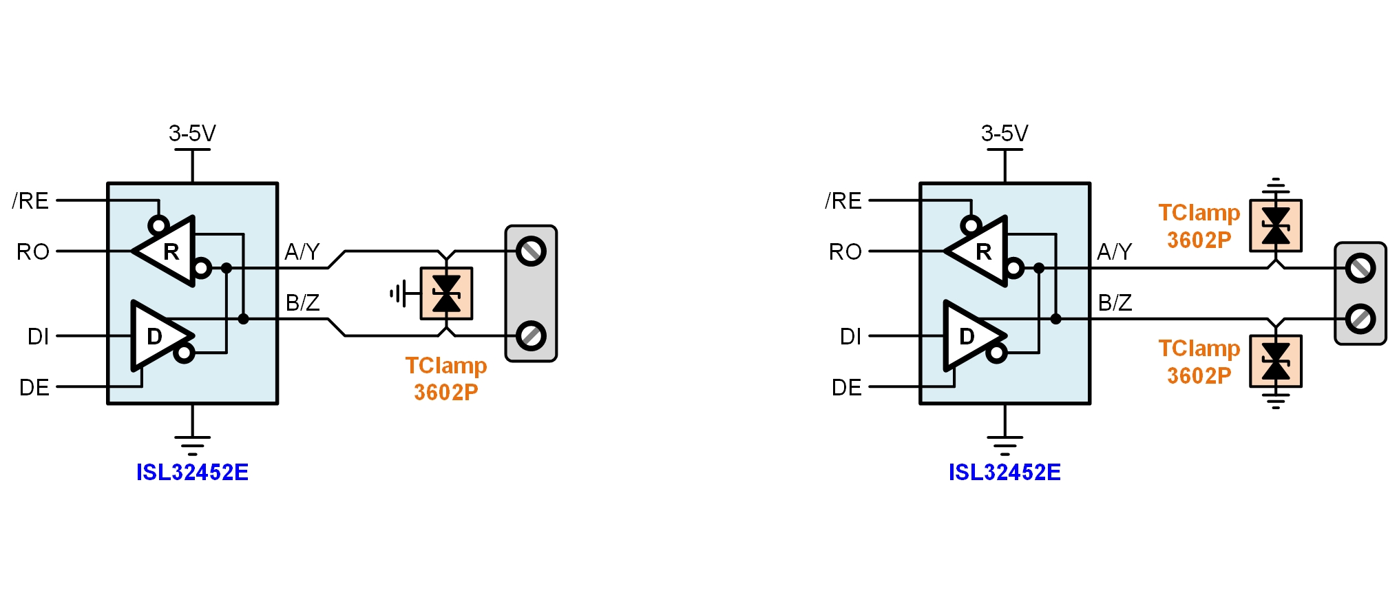 Figure 4: Lightning-protected RS-485 bus nodes.
There are several design option to proactively minimise the effects of over-voltage transients. The front and half times of ESD and EFT pulses are in the lower nanosecond range, leading to a frequency spectrum ranging from 30Hz up to 300MHz, turning the design of a robust over-voltage protection scheme into an RF design with requirements for decoupling and low-inductance returns paths.
It is important to ensure GND and VCC reference planes are true copper planes without holes or cut-outs. This ensures low-inductance return paths. High-frequency signals follow the path of least inductance, not the path of least impedance, which requires the use of multi-layer boards. Route signal traces are on the top layer, followed by the ground and VCC planes as second and third layers, respectively. Route control signals, such as the DE and /RE enable signals on the bottom layer.
The TVS should be placed as close as possible to the board connector to prevent transients from penetrating the board. Another tip is to design the data line traces to enable currents that flow easily into the TVS part before they proceed towards the transceiver bus terminals. Typical trace design uses small V-connections as shown in Figure 4, so the use of decoupling capacitors close to the supply terminals of the transceiver as well as other ICs is recommended.
It is preferable to use one capacitor value for decoupling and construct larger values through paralleling capacitors. The reactance of capacitors is first capacitive and later inductive, with increasing frequency. Using multiple capacitor values might cause the inductance of one cap-value to form an LC-tank with the capacitance of another cap-value, causing significant EMI.
Use a minimum of two ground vias for TVS devices and decoupling capacitors to minimise via inductance.
Conclusion
The combination of over-voltage protected transceivers, also called fault-protected transceivers, in combination with modern transient voltage suppressors simplifies over-voltage protection design cost, board space, and drastically reduces design and development time.
About the Author
Tom Kugelstadt is a principal application engineer with Renesas Electronics America where he defines new high-performance analogue products for industrial systems. He is a graduate from the Frankfurt University of Applied Science and has more than 35 years of experience in analogue circuit design.