


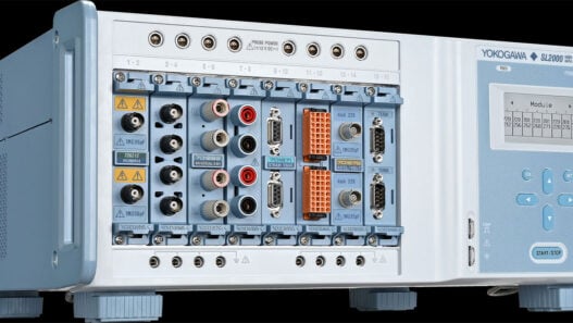

General part selection

Figure 3 – pre-booster schematic
Several components of the booster have an influence on achieving stable output voltage on a test pulse applied to the input. Let’s walk through the single components and their selection.
- The diode at the input prevents the input bulk capacitors C1 and C2 discharging when the test pulse is applied. As reverse polarity protection is needed in most cases, this functionality comes for free. A Schottky diode like Vishay SS5P5 (50V, 5A) has good performance and a decent package for distributing the losses.
- The bulk capacitors buffer the input voltage and reduce the falling slope of the test pulse. They have a big impact on performance. The maximum amount of capacitance is not only limited by space and cost, but also by the leakage current of the capacitors. As such systems are usually permanently connected to the battery, and a maximum quiescent current (mostly in the 100µA region per ECU) is specified, which does not only affect the boost controller itself but also its entire circuitry. Compared to the output, the input of a boost converter working in continuous conduction mode (CCM, inductor current never goes to zero) doesn’t see a large ripple current. It is a continuous current with a ripple on top. This means, the AC current stress for the input capacitors is low and inexpensive electrolytic capacitors with higher ESR and lower RMS current capability like Panasonic’s FK series can be used. The required voltage rating of the FET depends on the manufacturer. Some permit voltage peaks of 40.0V for 35V-rated capacitors, so a 50V-rated capacitor is not necessarily needed and should be checked with the manufacturer. The ISO 7637-2 standard defines pulses up to the 100V region. These pulses are damped at the battery mostly to 27V or 40V, but the damping is slow. So significant voltage peaks can be still present, meaning many OEM always demand capacitors with a voltage rating of at least 50V.
- Under normal boost operation, the FET sees a relatively low voltage but a high current. Unfortunately it has to withstand the 40.0V peak on the input, so a 40V-rated FET is needed, although boosting a 20V-rated device to improve performance would be sufficient. The 40.0V peak is applied on the input of the circuit and will be damped by the input filter as well as by the output capacitors, so it is not necessary to select a 60V-rated FET for additional headroom. Low resistance is more important than fast switching speed, since the currents are high and the voltage low. At the same time, care has to be taken of the total gate charge of the FET to avoid overloading the controller’s gate driver.
- The shunt resistor has to be small enough that the overcurrent protection is not tripping while the current peaks. It is important to know that calculation of the maximum current at minimum input voltage is not sufficient as this applies only for steady-state operation. As we will see later, the peak current will be much higher and it’s good practice to determine this value by measurement to avoid the overcurrent protection tripping too early.
- The inductor has to be selected so that it is able to handle the maximum current during the first part of the cranking pulse, while the battery voltage is dropping without going into saturation. Inductors made of composite material or iron powder like Coilcraft’s XAL series are good choices, because they have a high saturation current with soft saturation, low DC resistance and small size at the same time. A small disadvantage for this kind of inductor is the higher core loss compared to ferrite cores. But the large current stress is only present for a very short time, so this drawback can be dismissed. When checking the DC resistance of the inductor it has to be considered that while the booster is not switching the whole load current flows through it, causing additional losses.
- The average current rating of the diode between the switching node and the output capacitors is equal to the output current of 1.7A. Similar to the FET, its maximum blocking voltage has to be higher than needed for normal operation due to the possibility of a 40.0V peak on the input. When the booster is not switching and its output is loaded, this diode, as along with the reverse polarity protection diode, causes some losses. The thermal impact has to be considered when selecting the package of the diode. For convenience the same diode as for the reverse polarity protection has been used in this design.
- In opposition to the input, the output capacitors of a boost converter see large current ripple, meaning decent capacitance is necessary to smooth the output voltage. On a first glance, a high-quality low ESR (equivalent series resistance) electrolytic capacitor with high ripple-current capability is required. The current capability of a capacitor is mainly related to its ESR and its incorporated losses, which are the ESR multiplied by the square of the RMS value of the ripple current. A high ESR leads to higher losses and therefore higher temperatures inside the capacitor which have a negative influence on life time. In this application the booster is not working continuously but just for a relatively short time. So the average RMS value is much lower and an inexpensive electrolytic capacitor like that used for the input can be used. But that is not the whole truth. The booster supplies two buck converters, so the output capacitors of the booster are the input capacitors of the bucks. And in contrast to a boost, a buck converter has large ripple current on the input. So even while the booster is not switching, the output capacitors are still loaded with the large input AC current of the bucks. But if the booster output capacitors and the buck input capacitors are decoupled by a small inductor, a high ESR electrolytic capacitor can be used. A better approach is to use high-quality polymer hybrid capacitors like the Panasonic’s ZA series as the output capacitor for the booster and input capacitor for the bucks at the same time. This saves not only space on the PCB but can also reduce the total system cost as the buck input capacitors are not needed anymore. From a layout perspective, the buck converter has to be placed very close to the booster output capacitor in this case. For the test pulse, the output capacitor acts as an energy buffer. Obviously a large buffer will reduce the breakdown of the output voltage but similarly to the input capacitor, its capacitance is limited by the maximum leakage current.
The boost controller itself is supplied by its own output voltage. By doing this, the internal bias voltage is always on its nominal level of 8.0V and a no logic level FET for the power stage is needed. Besides that it offers the possibility to use the boost converter with input voltages below the minimum supply voltage of the IC.
Reaction of a booster on a test pulse
Figure 4 shows the waveforms of a typical pre-booster working in CCM during a test pulse. The green waveform is the input voltage, which follows the pulse described in Figure 1. Red is the voltage on the input capacitor behind the reverse polarity protection diode. The purple waveform is the output voltage of the booster and dark blue the inductor current with a significant elevation at first. The output of the boost controller’s error amplifier COMP is represented by the light blue trace on the bottom.

Figure 4 – complete cold start test pulse “severe” applied to a pre-booster
The purple boost output voltage shows a significant dip right at the beginning of the test pulse when the battery voltage drops from 11.0V down to 3.2V. After this event the output voltage is stable and well-regulated at 9.0V. So the most critical point for a pre-booster is to handle this large voltage drop without there being too large an impact and drop of the output voltage. The rest of the test pulse is pretty easy to handle and basically just a matter of thermal design. A closer look at the critical part of the test pulse is shown in Figure 5.

Figure 5 – beginning of the cold start test pulse “severe” applied to a pre-booster
The falling input slope is damped by the input capacitor (green trace). It takes approximately 1.2ms until the booster starts switching and the inductor current rises. Up to this point, the load is supplied only by the output capacitor and the output voltage is ramping down. Then the converter output starts to recover and settles at the nominal voltage of 9.0V.
In the following part we will discuss the reason for this behaviour in detail and how to improve it.
Impact of the error amplifier
The 1.2ms delay of the booster right at the beginning is caused by the saturation of the error amplifiers output (COMP). With 11.0V at the input the voltage on the feedback resistor divider is higher than the reference voltage. Thus the voltage at the error amplifier goes down to zero volts and the converter won’t switch. When the test pulse is applied, the output voltage drops and the feedback voltage goes below the reference voltage. Then the error amplifier needs to charge the capacitors of the compensation network (capacitors between COMP and FB / Pin 4 and 5) to a certain value needed for regulation. But the charge current is limited by the maximum output current of the error amplifier (250µA typical) and the resistor in series to the larger capacitor. This delay caused by the saturation of the error amplifier has the biggest impact on the breakdown of the output voltage during a cold start test pulse. The only way to mitigate this problem is to reduce the value of the capacitors and increase the resistor’s value. But this is not possible as these three components set the gain, one zero and one pole for the error amplifier to provide a well-regulated output, fast load regulation, as well as enough phase and gain margin. The bandwidth and therefore the gain of a booster working in CCM is practically limited by the right half plane zero. For a stable and reliable design, the maximum bandwidth is somewhere between one tenth and one fifth of this frequency.

The formula shows that the only possibility to influence this right half plane zero is the inductance, as all other parameters like output voltage, load current and duty cycle are given by the specification of the booster. When designing the compensation network it is important to consider the lowest frequency of the right half plane zero which occurs at the lowest input voltage and the maximum load. The bandwidth of such a pre-booster is typically in the range of some hundreds of Hertz up to several Kilohertz. Now, these conditions limit the bandwidth and result in specific values for the compensation network which cannot just be changed for improved test pulse behaviour without the risk of getting unstable over lifetime. A high bandwidth means large resistor and small capacitors in the compensation network, so the only way for a booster in CCM is to shift the right half plane zero to high frequencies by reducing the inductance. Then the output of the error amplifier can charge the capacitors faster and regulation starts earlier when a test pulse is applied.
The comparison in Table 1 shows the improvement regarding output voltage regulation if the bandwidth of the pre-booster is increased. The compensation network is adjusted such that the phase and gain margin are similar (at least 60° phase and -20dB gain margin). However the bandwidth is virtually doubled. Unless otherwise specified, all following measurements use a “standard” test setup. It uses an input capacitance of 220µF, an inductance of 2.2µH, an output capacitance of 47µF and the output voltage is set to 9.0V. The output is loaded with 10W by a LM53602-Q1 synchronous buck converter providing 5.0V at 2.0A.

Table 1 – doubling the bandwidth
With the bandwidth doubled, the breakdown of the output voltage is 26 percent compared to 58 percent with the lower bandwidth. The minimum voltage of 6.7V is well above the 5.0V output voltage of the subsequent buck converter and the system will work continuously and without interruption.
It brings a clear benefit to push the bandwidth of the pre-booster as high as possible, but sufficient phase and gain margin is still needed. Decreasing the inductance and thereby pushing the right half plane zero to higher frequencies offers potentially higher bandwidths and lower breakdown of the output voltage. Another benefit is the slightly lower inductor peak current. To understand this, a closer look at the output capacitor can help. While the input voltage is falling and the converter is not yet switching, the load is solely supplied by the output capacitor. As soon as the booster is switching, it needs to supply not only the load current, but also recharge the output capacitor. The lower the bandwidth, the higher the regulation delay, the higher the discharge of the capacitor and, as a consequence, the higher the current needed to recharge it.
The final part demonstrates the differences between operation modes and the influence of the inductance and capacitance on performance. Read part 3.