


Target applications cover centralised and string solar inverters, energy storage systems (ESS), industrial motion, electric vehicle (EV) on-board chargers, EV roadside fast chargers, wind energy, UPS, bi-directional microgrids, DC/DC converters, and solid-state circuit breakers.
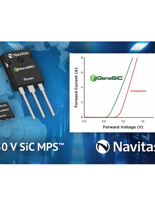
Ranging from 650 to 6,500V, Navitas has a wide range of SiC technology. From an original line-up of discrete packages – from 8 x 8mm surface-mount QFNs to through-hole TO-247s – the GeneSiC SiCPAK is an initial, direct entry point into higher-power applications. A comprehensive power-module roadmap, with high-voltage SiC MOSFETs and MPS diodes, GaN power ICs, high-speed digital isolators, and low-voltage silicon control ICs is being mapped out.
SiCPAK modules employ ‘press-fit’ technology to offer compact form factors for power circuits and deliver cost-effective, power-dense solutions to end users. The modules are built upon GeneSiC die that have already made a mark in terms of superior performance, reliability, and ruggedness.
Examples include a SiCPAK half-bridge module, rated at 6mOhm, 1,200V with trench-assisted planar-gate SiC MOSFET technology. Multiple configurations of SiC MOSFETs and MPS diodes will be available to create application-specific modules for superior system performance. The initial release will include 1,200V-rated half-bridge modules in 6, 12, 20, and 30mOhm ratings.
Within the lead-free SiCPAK, each SiC chip is silver (Ag) sintered to the module’s substrate for superior cooling and reliability. The substrate itself is ‘direct-bonded copper’ (DBC) and manufactured using an active-metal brazing (AMB) technique on silicon-nitride (Si3N4) ceramics, ideal for power-cycling applications. This construction delivers excellent strength and flexibility, fracture resistance, and good thermal conductivity for cool, reliable, long-life operation.
For customers who prefer to make their own high-power modules, all GeneSiC MOSFET and MPS diodes are available in bare die format, with gold (Au) and aluminium (Al) top-side metalisations.
Parts are available now to qualified customers.