


Ultra-low voltage devices are becoming mainstream in the industrial internet of things (IIoT), RF communication, energy harvesting and low-power wireless products. Most ultra-low-power efficiency networked systems also require ultra-low-voltage. These low voltage circuits, however, are at risk of over-voltage from transient voltage spikes from sudden load changes or high transient energy levels that can radiate throughout the system and cause damage.
Protection can take the form of either an over-voltage protection circuit or a voltage clamp, which is a circuit designed to limit the output voltage to a specific range.
These options monitor the input voltage and control the external transistor switch’s gate without affecting the load circuit’s operation. The over-voltage protection circuit, however, disconnects the load during the transient event, whereas the voltage clamp continues to load power.
Using simple diodes as voltage clamps is not always practical as they have limited forward voltages and power-handling capabilities. Low voltage Zener diodes have high leakage currents and imprecise voltage ratings. Yet, metal oxide varistors (MOVs), and most transient voltage suppressor (TVS) devices, are also impractical, as they have breakdown voltages greater than 5.0V.
Voltage protection
Advanced Linear Devices (ALD) provides voltage protection using very low-voltage precision enhancement-mode MOSFETs to improve the clamping compared to Zener diodes. Figure 1 shows a circuit designed to simulate a low-power Zener shunt regulator using two parallel-connected Electrically Programmable Analog Device (EPAD) transistors.
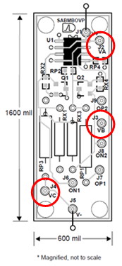 Figure 1: the pinout of a typical ALD clamp.
ALD’s EPAD technology was developed for low voltage, low power, high precision linear circuit applications. The CMOS-based device is combined with an inexpensive programmer and allows software-based analogue circuit trimming in up to 100,000 discrete steps with resolution as low as 0.1mV.
Each EPAD contains MOSFET transistors with programmable threshold voltages. The set voltage and current levels are stored indefinitely, even when the power is removed. Unlike microcontroller-based trimming, the EPAD does not require additional circuitry but does use a fraction of the power and less board space than a microcontroller solution.
The company’s low power precision voltage clamping devices also provide excellent low-voltage control in applications where the clamping voltage is 5V or less. For example, the SABMBOVP216 can operate down to 1.6V.
Compared to a Zener diode clamp, this circuit, at less than 100nA (maximum), has a much lower quiescent current than the low voltage Zener. It also has a better voltage-versus-current (I-V) characteristic and more precise voltages than the Zener alternative. Another benefit is response time, which at less than 100 ns is better than when using a Zener diode. In addition, the surge current handling capability is better at greater than 2.0A.
It may be necessary for higher voltages (5.0 to 10V) to stack two or more EPAD devices. The designer must take care to ensure voltages remain low; a TVS across supply rails is recommended.
Figure 1 illustrates the pinout of the ALD clamps. Most of the pins are left open; only pins VA, VB, and VC are connected in this application. Each device provides two identical clamp voltages. One is between VB and VC; the other is between VA and VB. These can be used as independent clamps as long as the VB level of the VA-B clamp is the same as the VB level of the VB-C clamp.
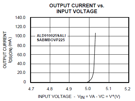 Figure 2: Clamping current as a function of input voltage for two stacked 2.5V clamps.
The low-voltage operating limit is determined by the upper threshold voltages, either the EPAD transistor or the p-channel power MOSFET, plus an overdrive voltage to attain a pre-selected current clamp level.
Stacking various EPAD transistors can realize different combinations of clamp voltages.
In addition to clamping voltages is well below anything achievable by a Zener diode, the ALD overvoltage protection (OVP) clamps do not require the additional components, such as a resistor divider, amplifier buffering circuits, and voltage regulator circuits. The ALD clamping method reduces complexity, saves costs, and lowers power consumption.
Each ALD clamping device provides two identical clamp voltages (Figure 2). The clamps can be used independently or stacked, doubling the clamping threshold. There is a sharp turn-on at 5.0V.
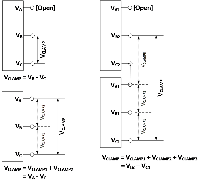 Figure 3: Examples of single and double clamp circuits.
Figure 3 show a single clamp (top left) and a stacked clamp (right). The single clamp must be between VB and VC with VA left open. For the circuit below (bottom left), the basic clamp level is doubled by stacking VCLAMP1 and VCLAMP2.
Using very low voltage, precision enhancement-mode MOSFETs can not only improve the design of voltage clamps for low-voltage applications to offer protection, but they can also extend the usefulness of ultra-low voltage designs.
The author:
Robert L Chao is President and CEO of Advanced Linear Devices (ALD). He holds BS and MS degrees in Electrical Engineering from UC Berkeley and has been a leading authority in the analogue semiconductor industry for over 30 years.