


A quasi-resonant flyback is simply a discontinuous current mode (DCM) flyback with a valley switching turn on. It is also known as variable frequency or valley switching flyback and is largely used in low power switch mode power supply application such as charger, adapter and auxiliary supply.
This article presents an ultra-wide input voltage range flyback which works in quasi-resonant (QR) mode and is primary side regulated. A primary side regulated topology uses the magnetic feedback via the bias winding to close the feedback loop. The bias winding is needed to provide the supply voltage for the controller. Cost is minimised as a simple resistor divider is sufficient to get the information from the bias winding to regulate the output voltage. The other advantage is that the QR operation gives the best possible efficiency because it uses the resonance ringing, caused by the circuit parasitics, to lower the switching losses. Usually, a fixed frequency controller is used for a wide input voltage range.
Voltage rating of input capacitor
The reference design PMP10200 shows that an efficient and cheap primary side regulated QR flyback topology also works for an ultra-wide input.
A small input capacitor results in a low bulk voltage and high peak currents. A large input capacitor is more expensive. A good compromise is to use a capacitor value that limits the voltage ripple to about 30%. The capacitor must be rated for the input ripple current and the maximum input voltage. If used for an offline application, the physical size of the capacitor is large because of the very high input voltage.
Consider a wide input voltage design with a maximum voltage of 520V. Usually an aluminium electrolytic capacitor does not withstand a voltage higher than 450V. Two capacitors in the series must be taken, and usually an additional resistor divider in parallel to the two capacitors is needed to ensure equal voltage sharing. A flyback controller needs a start-up circuit for high input voltage applications. The resistors of the start-up circuit can be used to provide an equivalent voltage shared between the input capacitors. The voltage rating of a surface mount resistor is limited, therefore it is recommended to use some in series.
Startup circuit
The resistive start-up method results in an increase in standby losses. An active start-up method is recommended for low standby power applications. Some controllers can integrate the start-up FET, but if the voltage rating of the internal FET is too low, then a controller without this must be used. An external startup circuit can provide the low standby power function in this case. The TI reference design PMP10200 shows an optional start-up circuit (marked yellow). This circuit contains a normally on high voltage device, in this case it is the depletion mode MOSFET Q1, that supplies the charging current for the VDD capacitor C12. Once the controller has started switching, the voltage of the bias winding will turn the depletion mode MOSFET off. When the controller starts switching, the capacitor C11 will be charged, and the capacitor voltage VC11 increases. As VC11 exceeds the threshold voltage, the small MOSFET Q2 turns on which pulls down the gate-to-source voltage Vgs_Q1 of the MOSFET Q1 to a negative value. Q1 turns off and, as a result, the power dissipation of the startup circuit decreases to a very low level.
Flyback voltage
The reflected output voltage, referred to as the flyback voltage, is defined as Vflyback = (Vout+ Vdiode) x turns-ratio. Many designers select Vflyback based upon the voltage stress of the primary MOSFET, but there are some trade-offs. A high Vflyback will result in lower switching losses but will increase conduction losses because a high voltage MOSFET is needed. A high voltage MOSFET will be more expensive and will have a higher RDS (on) compared to a MOSFET rated for lower voltages. A good method for a universal input (85 to 265V AC) is to choose Vflyback as high as the minimum bulk input voltage. This will result in zero voltage switching for low line, and reduced switching losses for higher input voltages. For a wide input voltage range however, the minimum input voltage is very low. The advantage of the valley switching is negligible if a very low flyback voltage is chosen.
If the flyback voltage is much higher than the input voltage, the drain-to-source voltage VDS will swing down to a level as low as the bulk input voltage minus the flyback voltage. If Vflyback is less than VIN, minimum the voltage VDS will swing down to a level lower than zero volt and will be clamped by the body diode of the MOSFET. The short conduction of the body diode will generate additional losses but usually they are not very high. As long as the temperature of the MOSFET does not get too high for the application, it is not a problem.
Primary inductance
There are different modulating techniques for QR flyback controllers. A primary side regulated controller (like UCC28700) modulates the primary peak current or the switching frequency, but not at the same time (see Figure 2). The primary current, the turns-ratio and the primary inductance define the operating mode and limit the maximum switching frequency. To define the optimal primary inductance for this kind of controller, first consider if a maximum frequency limit is desired. Secondly determine the conditions where the controller should work in QR mode. During QR mode the frequency varies in order to have the switching event happen on the first resonant valley that occurs after the demagnetising of the transformer. After the secondary side current has ramped down to zero (core is completely demagnetised) there will be a resonant ringing, caused by the primary inductance and the energy stored in the parasitic capacitances. The controller detects the valley of the resonant ringing and turns on the MOSFET. The lower switch node voltage at the valley reduces the switching losses. Switching at the first valley is called QR mode where the voltage is at the lowest value and, therefore, the highest efficiency is achieved. The primary inductance defines the conditions where the controller works in QR mode.
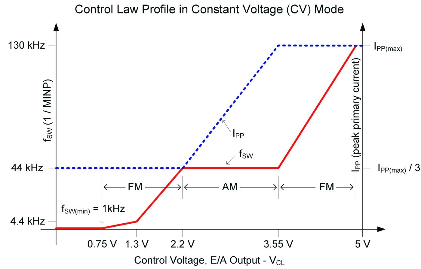
Figure 2: Frequency and amplitude modulating modes
A good starting point is to select the primary inductance, so that the controller works in QR mode for the nominal input voltage. This is because it is usually the most commonly occurring operating condition. Follow this simplified equation to calculate what is primary inductance is needed for the quasi-resonant mode.
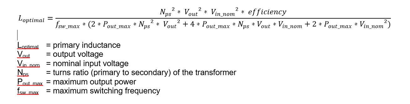
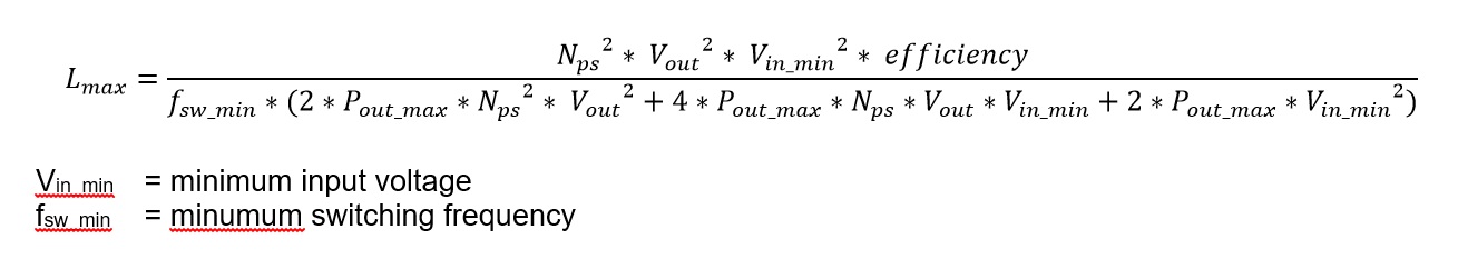
Note that the inductance must be lower than Lmax (see equation below). A higher value is not able to deliver the full output power at the minimum input voltage and at the minimum switching frequency fsw_min. fsw_min (= 44kHz for the UCC28700) is the minimum possible frequency during frequency modulation mode with maximum primary peak current.
Calculation example
A practical example of the reference design PMP10200 is given below. The maximum switching frequency (fsw_max=130kHz) of the PMP10200 should not be limited. For the nominal input voltage of 150V and the maximum output power of 20W the controller should work in QR mode. Equation 1 calculates an inductance of 280µH.
The controller must be able to deliver the full output power for the very low input voltage of 25V. Considering the minimum frequency of 44kHz, the maximum allowed inductance is 150µH (Equation 2). An additional safety margin must be adhered to this value. With an inductance of 100µH the controller is able to deliver the output power over the full input voltage range, but unfortunately the design will always work in discontinuous mode, never in QR mode.
Using the formulas for defining the primary inductance will lead to an optimal performance. It is recommended to specify the inductance in this way so that the controller is not working too deep in DCM mode, if it is not possible to work in QR mode. Therefore, the controller will switch at a later valley, where the voltage is in fact higher than at the first valley, but the advantage of valley switching still exists.
Figure 3 (below) shows the PMP10200 efficiency for an input voltage of 150V. The peak efficiency is about 89% for a large output power range.
