Silicon is the base material for almost all modern electronics. It is an abundant material. It has ideal electrical properties. It is cheap to process. And it has been the backbone of chipmaking for decades. But it is running out of room to grow.
Transistors can only be shrunk so far before heat, leakage, and physical limits begin to outweigh gains. For applications like AI, quantum, robotics, and Edge systems, that ceiling is already visible. Jiadi Zhu, Founder and CEO at CDimension, believes the answer lies not in pushing silicon harder, but in rebuilding the material base entirely.
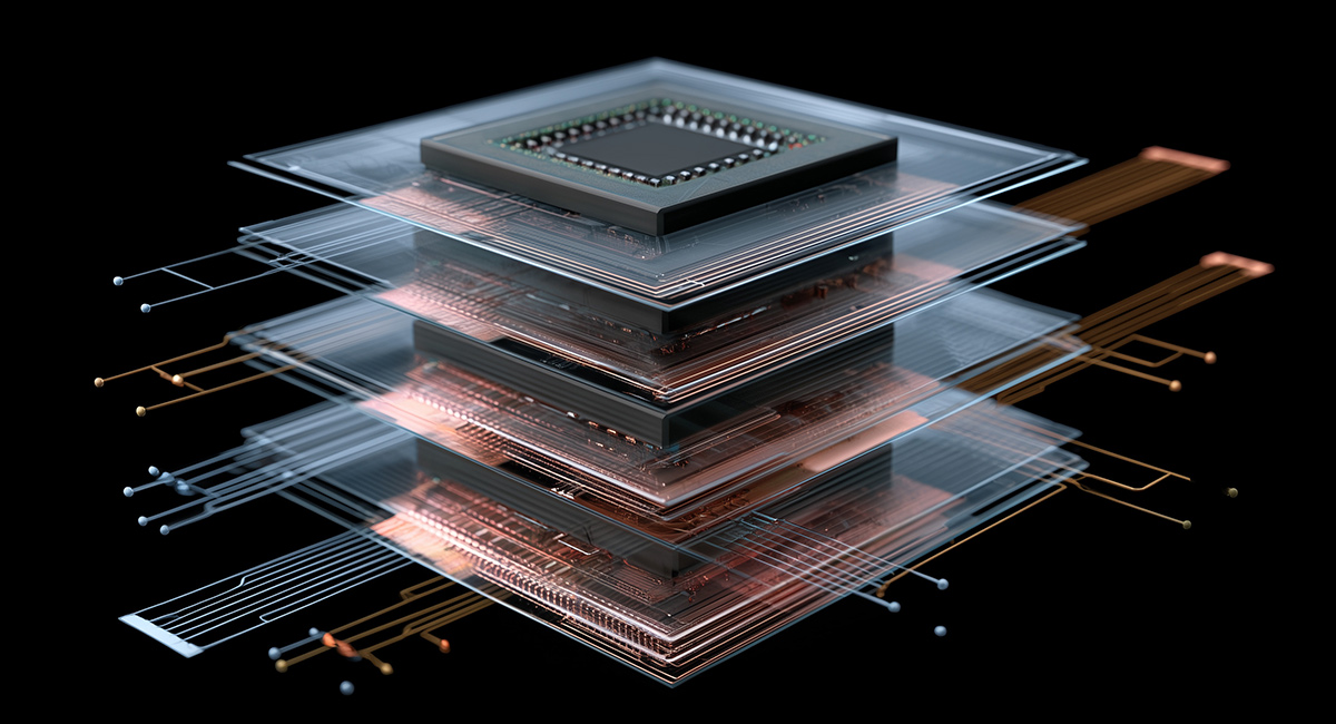
The company is developing wafer-scale, atomically thin 2D materials that can be integrated directly into today’s semiconductor workflows. These layers are only a few atoms thick, smooth enough to stack, and use far less energy.
Why silicon is no longer enough
Moore’s Law has relied on shrinking silicon-based transistors, but silicon’s physical limits are becoming harder to work around. As devices shrink, traditional silicon causes more leakage, resistance, and power loss, making it increasingly difficult to maintain performance and efficiency at smaller scales. These limits put a cap on performance in data centres and devices that overheat easily.
Realising that “the real bottleneck wasn’t in design, it was in the materials,” is what drew Zhu to 2D materials. “Silicon alone can no longer keep up with the demands of AI, quantum computing, robotics, and Edge systems,” said Zhu. With this in mind, CDimension’s work takes a materials-first approach.
“Our 2D materials make chips both faster and more energy-efficient because they solve the problem at its root: the materials. Silicon is thick, so signals have to travel longer distances … Compared to silicon, our materials are atomically thin, 100,000x thinner.”
That thinness translates directly to lower energy use, reduced leakage, and shorter interconnects. The company reports up to a 1,000x improvement in transistor-level energy efficiency compared with silicon, achieved through full-wafer growth of uniform semiconductors and insulators.
A breakthrough in wafer-scale 2D materials
For decades, 2D materials promised new possibilities but remained trapped in laboratory-scale samples. CDimension’s core breakthrough is the ability to grow high-quality 2D semiconductors and insulators uniformly across full wafers.
“The breakthrough is that we can now produce wafer-scale, high-quality 2D materials … supporting dense vertical stacking and enabling new levels of integration.”
The emphasis is on compatibility. Rather than asking foundries to adopt unfamiliar processes or invest in new facilities, CDimension aligns its approach with existing tools.
“In short, our integration process is fully silicon-compatible. We’re extending the roadmap of chipmaking, which means not replacing silicon overnight but building the next layer on top of it.”
Why this matters for AI
AI systems demand increasingly complex models that strain power budgets. Density and heat are limiting factors, and both stem from the physics of silicon. CDimension materials address this at the source.
“AI workloads push chips to their limits in both power and density … Our 2D materials reduce leakage and power draw, which means AI hardware can run larger, more complex models without overheating or hitting power walls.”
For data centres, mobile devices, and Edge hardware, this could mean more capability without an equivalent rise in energy use.
Tackling quantum’s toughest challenge
Quantum computing faces a different bottleneck. Qubits are sensitive to noise, and even minor defects in the underlying material can interrupt or degrade operations. Error correction depends on long coherence times, and today’s materials struggle to support these reliably. CDimension’s single-crystalline 2D insulators are designed to minimise noise at the materials level.
“Qubits are so fragile that the smallest physical defect or thermal disturbance can cause them to lose information … We produce single-crystalline 2D insulators that dramatically reduce noise and extend qubit coherence time.”
This could support more reliable qubit interconnection and help quantum systems scale beyond the lab.
Building a hybrid future
While different in their needs, AI and quantum both face fundamental material limits. CDimension’s long-term vision is a hybrid computing future, enabled by materials designed for efficiency, stacking, and noise reduction.
“I truly believe that the near future of computing will be hybrid, where semiconductors and quantum coexist … we’re removing the materials bottleneck so conventional chips can stack higher and quantum qubits can stay quieter.”
This vision depends on manufacturing practicality. CDimension’s approach focuses on producing reliable, reproducible materials that work at the wafer scale and integrate into existing foundry lines. Customers, including research teams at Duke and UCSD, are already using the materials directly in device and circuit development.
Challenges and lessons learned
Moving from laboratory theory to large-scale production required years of process refinement: “Material quality, reproducibility, and contamination control are among the most important factors … We’ve spent over five years developing our process and equipment to ensure good quality and uniformity.”
Partnerships across research and industry have given CDimension valuable feedback, guiding improvements in “recipe tuning, design, and optimisation,” said Zhu.
What comes next
Looking to the future, CDimension sees itself not as a replacement for silicon but as a way to extend computing beyond its current limits. Zhu summarised the shift as building with pages rather than bricks: thin, smooth, and ready to stack.
“Think of it like this: trying to build the future of chips with silicon alone is like trying to make a book out of bricks. It worked for a long time, but now the bricks are too bulky to stack any further. Our 2D materials are like pages – ultra-thin, smooth, and stackable. From there, we can build the books (integrated circuits), and eventually even the writing inside (applications like quantum computing).
“For decades, progress in computing has depended on squeezing more out of silicon. What we’re doing is rebuilding that foundation so the next wave of innovation … has room to grow.”
The company frames its mission as simply to make materials that work in the real world. If successful, the next generation of AI, quantum, and hybrid systems may be defined less by transistor counts and more by the layers of atom-thin materials beneath them.