


This article originally appeared in the December’24 magazine issue of Electronic Specifier Design – see ES’s Magazine Archives for more featured publications.
To learn more, Harry Fowle, Associate Editor at Electronic Specifier, spoke with Michael Sorger, Project Lead for 300mm GaN at Infineon Technologies.
The transition from 200 to 300mm
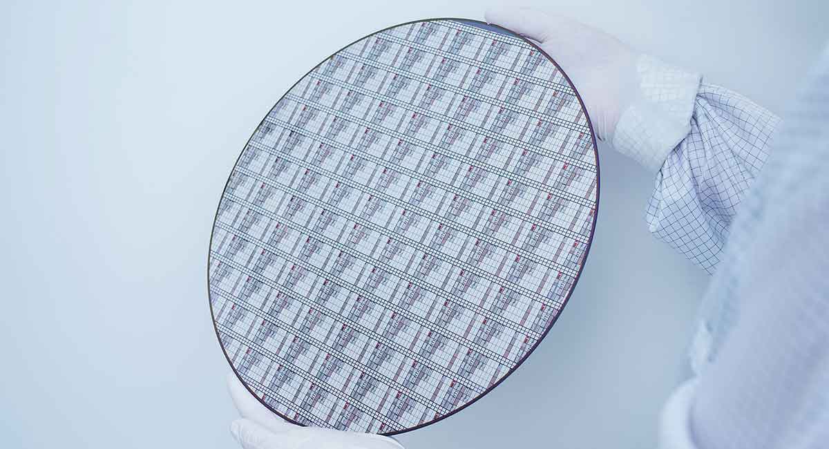
Transitioning from 200mm GaN wafers to 300mm is no easy feat, scaling up wafer size introduces a plethora of challenges such as maintaining material quality and uniformity across larger surfaces, mitigating increased risks of warping and defects, and addressing thermal management complexities owing to GaN’s high thermal conductivity.
Infineon recognised these challenges, as Sorger explained: “One of the key challenges in GaN manufacturing is to grow a homogenous GaN layer on top of the Si substrate (epitaxy) as the lattice mismatch between GaN and Si creates substantial stress in the material. The bigger the wafer diameter, the bigger this challenge becomes. For GaN on a 300mm Si wafer, this stress is as high as four elephants weighing 5 tonnes each sitting on a €1 coin.”
To overcome this, the team at Infineon had to develop its own IP for the GaN epitaxy field.
Achieving cost parity with silicon
One of the main goals with this new development is to achieve a cheaper GaN product and ideally reach cost parity with silicon.
Sorger explored Infineon’s position on this: “Fully scaled 300mm GaN production will contribute to GaN cost parity with silicon on RDS(on) level, which means cost parity for comparable Si and GaN system solutions. We will scale GaN capacity within our already existing large-scale silicon footprint according to market needs.”
The RDS(on) levels achieved through increased chip density utilising this new technology are enabling 2.3 times more chips per wafer. Infineon are also able to leverage existing 300mm silicon manufacturing infrastructure to keep costs as low as possible. Economies of scale from fully scaled production further reduce costs, making GaN competitive with silicon. This parity is projected to be achieved as production scales and the market grows, with full realisation anticipated by the end of the decade.
Industry impact
Infineon’s 300mm GaN technology is expected to significantly impact industries across various sectors. “GaN based power semiconductors find fast adoption in industrial, automotive, and consumer, computing & communication applications, including power supplies for AI systems, solar inverters, chargers and adapters, and motor-control systems,” enthused Sorger.
The technology’s efficiency, compact size, and performance improvements enable more effective and scalable solutions, addressing the needs of these sectors while benefiting end users with cost-effective and high-performing products.
A greener future in mind
For some time now Infineon has had sustainability and decarbonisation as a central part of the company’s development, and this hasn’t stopped with the development and scaling of 300mm GaN technology.
The technology directly supports energy-efficient solutions across industries like renewable energy, automotive, and industrial systems by enabling smaller, lighter, and more efficient devices.
“Wide bandgap materials like GaN or silicon carbide (SiC) have many advantages in terms of energy efficiency and thus make an important contribution to decarbonisation. At Infineon, we currently see green mobility of the future and the transition to renewable energies as two of the strongest growth drivers for our business in general, contributing to our scaling efforts of wide bandgap technology,” says Sorger.
The integration of GaN into existing silicon manufacturing infrastructure further minimises resource use and capital expenditure, aligning with Infineon’s strategic mission to drive decarbonisation and digitalisation globally.
Scaling with the market
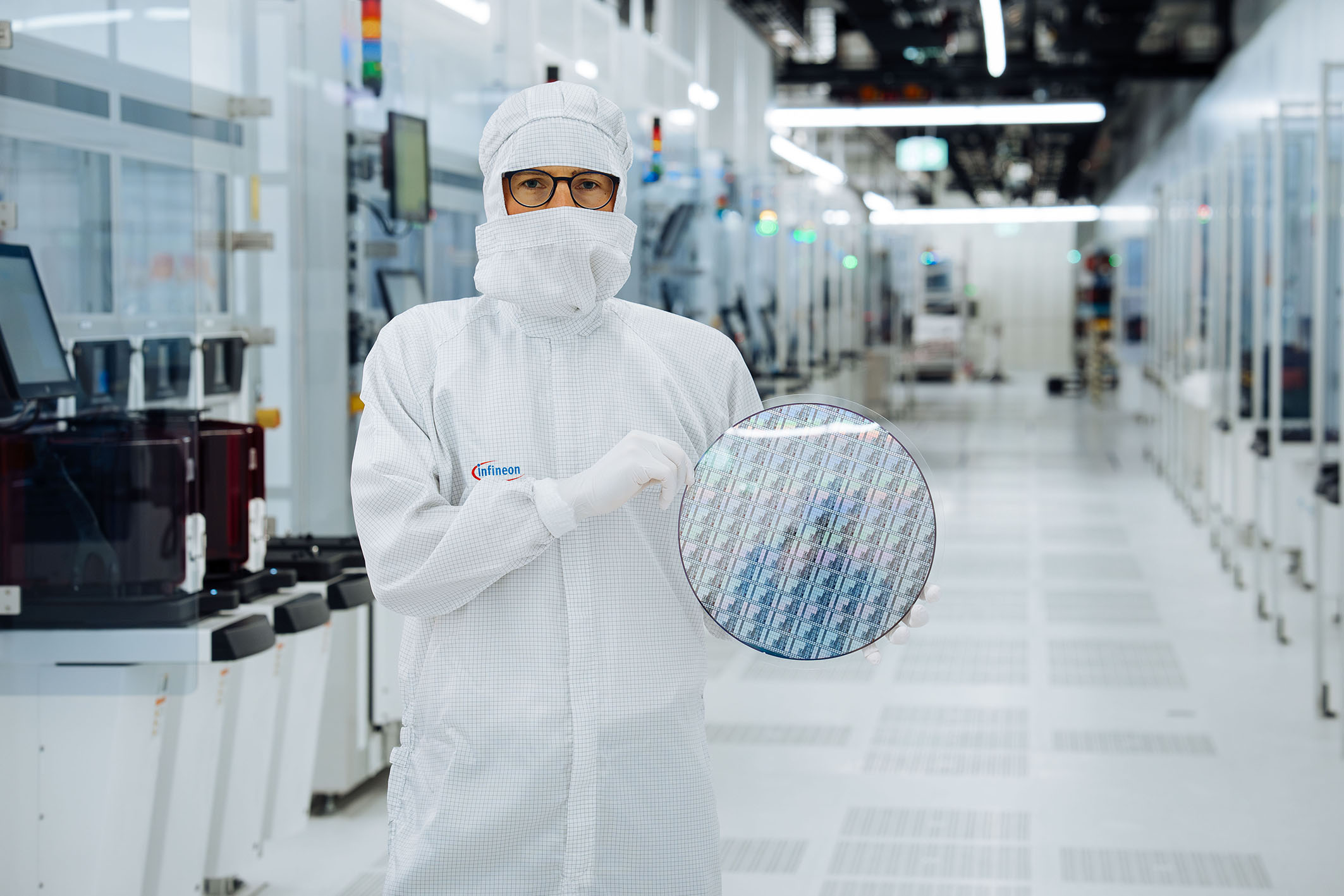
Infineon is well aware that the market for GaN is a growing one and is ready to scale as demand for its GaN semiconductors increases. Comments Sorger: “We have succeeded in manufacturing 300mm GaN wafers on an integrated pilot line in the existing 300mm silicon production in our Global Competence Centre for Wide-Bandgap and Power Semiconductors in Villach, Austria.”
By integrating GaN production into its proven 300mm silicon lines, Infineon can ensure supply stability while accelerating implementation to meet the growing demand, with the GaN market projected to reach several billion US dollars by the end of the decade.