


Next generation IGBT7
The seventh generation of IGBT power modules are now available in seven packages across multiple parts. These devices feature lower VCE (sat) and VF, overload capacity at TJ of 175°C, 50% higher current capability, enhanced controllability of dv/dt, improved FWD softness, and simpler driving compared to previous legacy generations. These features offer a differentiated value proposition of high-power density, durability, reduced system costs, higher efficiency, ease of use, and faster time to market.
IGBT7 portfolio
IGBT7 power modules are available in the industry-standard 62mm packages for phase leg or half bridge configuration in D3 package and for single-switch configuration in D4 packages. Microchips offer low-inductance/low-profile packages in 62mm, such as SP6C, SP6P, and SP6LI, offer reduced profile height and lower package inductance and enable high-power density with high reliability. Lower power levels can be served with smaller packages such as SP1F and SP3F, which are also low-profile packages available in various configurations. The ratings extend up to 900A with 1200 and 1700V.
Lower on-state voltage VCE (sat) and lower Vf with improved FWD
With 15 to 20% lower on-state voltage, there is significant loss reduction up to mid switching frequency applications, while the conduction losses at the given dv/ dt limitation are decreased and there is a reduction in antiparallel diode loss.
Conduction losses of the IGBTs are directly proportional to the VCE (sat) of the IGBT technology. The reduction of VCE (sat) reduces the conduction losses significantly and in turn enhances the efficiency of the converter.
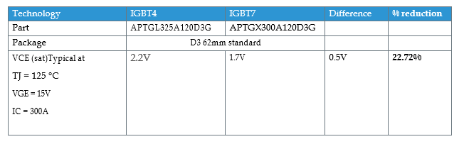
Table 1: an example comparison between IGBT4 and IGBT7 specs Vce (sat)
Overload capability at TVJ (op) is 175°C
The maximum junction temperature of 175°C compared to 150°C (IGBT4) is key for motor drives for repetitive, short term overload operation. The IGBT7 power modules are built for challenging applications as they can withstand junction temperature of 175°C during overload condition as opposed to 150°C for IGBT4. This 25°C improvement not only has tremendous advantages in the reliability and durability of the drive power inverter but also can result in cost-saving benefits with the high-performance-to-cost ratio of the IGBT7 over any other technology.
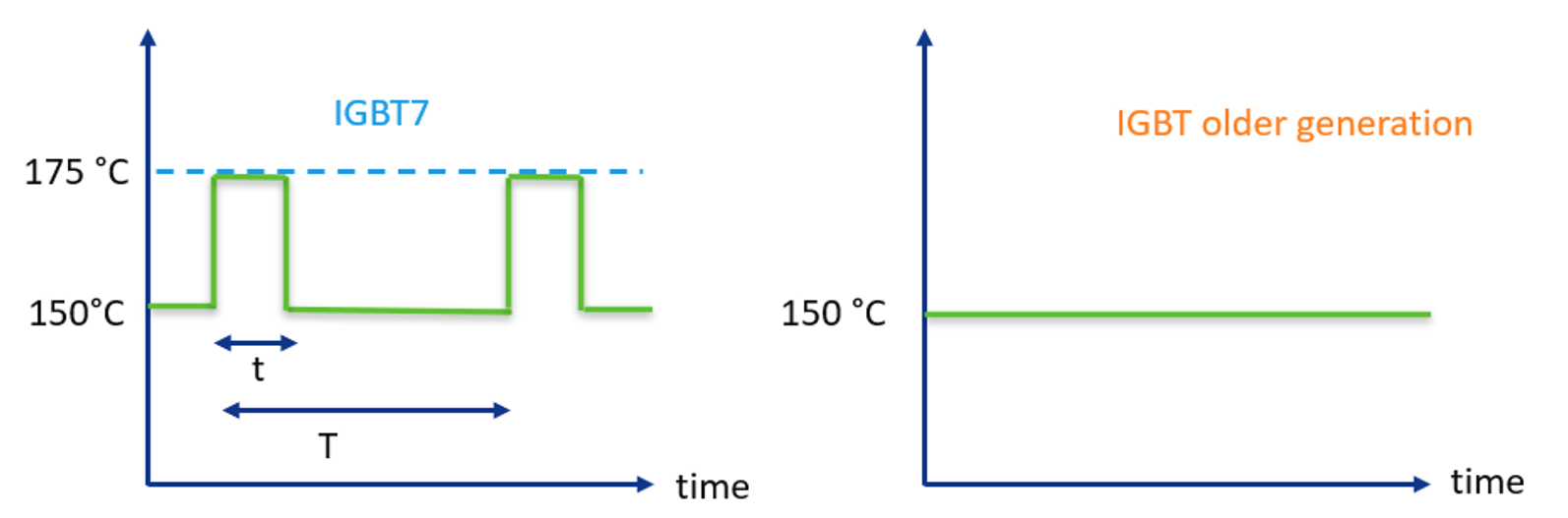
Figure 1: maximum operation junction temperature comparison between the IGBT7 and older IGBT generations
Enhanced controllability of dv/dt
Inverters are used to drive the motor, Pulse-Width Modulation (PWM) signals do not produce sinusoidal output voltage waveforms. This higher pulse rise time of the switches due to switching frequency results in high dv/ dt, which is further exacerbated by the long cables used in the motor drive application from the inverter to the motor, resulting in higher peak voltages right at the motor terminals. Longer motor cables even result in higher voltage overshoot with peak values as high as five times the system operating voltage (> 2000V for 415V systems). High voltage spikes can lead to insulation breakdown, resulting in phase-to-phase or turn-to-turn short circuits, with subsequent over-current trips by the drive sensor.
This is why motor manufacturers strongly recommend not exceeding the dv/dt of 5kV/µs at the inverter terminal in the worst-case scenario for 3-phase motors of typical 380/415/440 VAC. It is important to optimise the voltage gradient dv/dt as per the motor insulation requirement while carefully designing the general-purpose industrial drive.
To achieve this optimisation, IGBT7 demonstrates the highest level of perfection in controlling the inverter’s ability to change the dv/dt through adjustment of gate resistor (Rg).
Simple and hassle-free gate driving
CGE (Gate Emitter Capacitance) and CGC (Gate Collector capacitance) are balanced to give the IGBT7 full control over the dv/ dt, and to optimise the switching waveform and CGE is designed to avoid parasitic turn-on effects, so zero voltage supply for turn-off is feasible (unipolar gate driver power supply).
Higher current capability
The IGBT7 chip inherently has more current capability than the previous generation IGBT4. This results in higher output power for the given footprints, resulting in frame size jump, which implies a lower frame size can be used in lieu of bigger ones. This also increases the overall power density as more power can be compressed in a given area, avoids paralleling of number of switches, reduces the complexity, and improves reliability and durability. Higher power density reduces the power system Bill of Material (BoM) costs and offers faster time to market.
Lower inductance and lower profile packages
Microchip’s low parasitic inductance packages reduce the voltage overshoot, and enhances the durability and reliability. Lower profile enables packing more power in less volume improving the power density when used with IGBT7 technology.
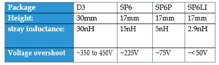
Table 2
The IGBT7 features and its end user benefits make these power modules versatile for multiple applications and megatrends from low to mid switching frequency applications. The ease of use without complexity in gate drive mechanism makes the design hassle free and obviates the resources in designing new drivers. The multiple topologies can be readily used as building blocks for converters of multiple applications providing design flexibility and faster time to market.
References:
https://www.fluke.com/en-us/learn/blog/power-quality/cable-length-vfd-motors
Application Manual Power Semiconductors (Semikron)
TRENCHSTOP™ 1200 V IGBT7 T7
Application Note (Infineon) (AN2018-14)
Amit’s Tech Corner, Microchip Aviation and Defense Newsletter Edition 23 Dec 2024
By Amit Gole, Product Marketing Manager for Microchip Technology’s integrated power solutions
This article originally appeared in the May’25 magazine issue of Electronic Specifier Design – see ES’s Magazine Archives for more featured publications.