


A high power 1/16th brick converter using GaN FETs could increase maximum load current in 1/16th brick converter designs, compared with MOSFET designs, explain Yuanzhe Zhang, director, applications engineering, Michael de Rooij, vice president of applications engineering, both Efficient Power Conversion and Andreas Reiter, director, applications engineering, digital power supplies, Microchip Technology
Brick DC/DC converters are widely used in data centre, telecommunications and automotive applications, converting a nominal 48V to different output nominal voltages such as 5.0, 9.0 and 12V. The main trend has been towards higher power density given a fixed form factor.
This article focuses on a 48V input to 12V maximum output, 300W converter design with output current capability up to 25A presented with peak efficiency of the converter of 95% and maximum power density of 730 W/in3. With 2µF extra input capacitance, the peak efficiency can reach 95.8%.
The standard dimension of the 1/16th brick converter is 33 x 22.9mm (1.3 x 0.9 inch) and the height limit is 10mm (0.4 inch).
Design challenges
The key challenge for a high power density 1/16th brick is magnetics. Due to space and dimension constraints, the magnetics are limited in size and shape. In addition, high output current (up to 25A) requires high saturation current rating, but inductors with high saturation current are usually bulky. A two-phase synchronous buck topology can be used so that two inductors share the output current and therefore the peak current requirement can be reduced. The simplified schematic is shown in Figure 1.
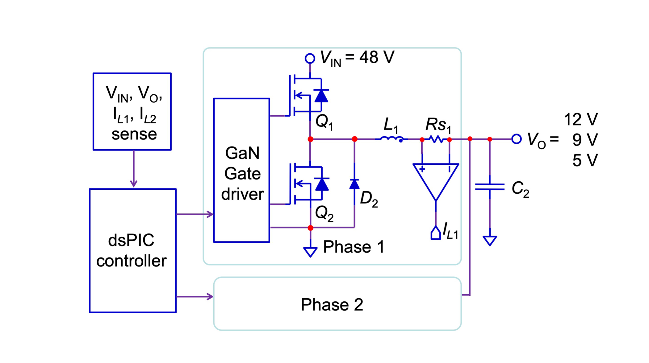 Figure 1: Simplified schematic diagram of the 1/16th brick converter
The second challenge lies in the selection of switching transistors. The transistors need to have a very good hard switching figure-of-merit and a small footprint, since the magnetics occupy a significant amount of board space. In this project, 100V GaN FETs (EPC2053) in a chip scale package were selected to meet these requirements.
The next challenge is the lack of GaN-compatible controllers. Off-the-shelf MOSFET controllers usually have long dead times (in excess of 20ns), a slow and damped gate driver and are unable to handle negative voltages of -2.0 to -3.0V at the switch node. As a result, circuit adaptations of MOSFET controllers are required to ensure proper operation that come at the expense of efficiency. In this design, a dsPIC33 microcontroller was used to exploit the high performance of GaN FETs.
Power stage design
The synchronous buck converter is selected as the base topology. Considering the maximum output current of 25A, if a single inductor is used, its current rating needs to be at least 33A, assuming 30% peak-to-average current ripple. Inductors that satisfy this requirement will not fit under the height limit. In a two-phase synchronous buck converter, each inductor only conducts 12.5A DC current. With 30% ripple, the peak current is 16.25A.
eGaN FETs with 3.2mΩ RON are used in order to reduce the converter size and conduction loss. The GaN-specific gate driver, uP1966A from uPI semiconductor was also selected. This eliminates the need for an anti-parallel diode (D2 in Figure 1), and reduces loss.
To take advantage of the fast switching of eGaN FETs, the power loop inductance needs to be minimised. The second layer of the PCB is a ground plane. Another two layers of ground plane are also included in this six-layer PCB, for better heat sinking.
TDK B82559 series inductors are good options, with dimensions of 13 x 10.7mm (0.51 x 0.42 inch), and a height of 5.0 or 6.0mm. They also have high saturation current rating and low DCR. The 2.4µH inductor has a saturation current rating of 16.5A. Selecting 500kHz switching frequency results in 16.25A peak current under nominal operating condition that satisfies the saturation current requirement.
Digital control
A dsPIC33CK digital controller was used to address the controller compatibility issue. The 16-bit processor has a maximum CPU speed of 100MIPS. The pulse width modulation (PWM) module can be configured in high resolution mode, resulting in 0.25ns resolution in duty cycle and dead times, allowing accurate adjustment of dead times.
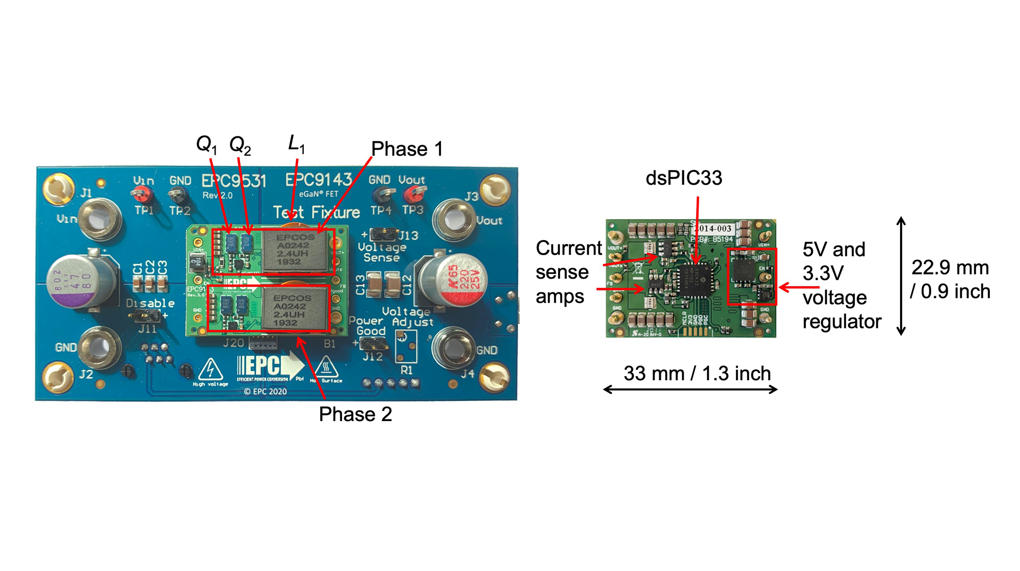
Figure 2: 1/16th brick converter EPC9143 mounted on the EPC9531 test fixture (left) and bottom side of the converter
There are two options for the digital control loop, either a multi-loop controller or single voltage loop with phase current balancing. Both options require current sensing circuitry, consisting of sense resistors and differential amplifiers. In this design, 1mΩ sense resistors and low-noise amplifiers MCP6C02 were used. The multi-loop controller uses a single voltage loop providing the same current reference (IREF) to the two independent inner current loops. As a result, the current in both inductors will be regulated to the same value. The bandwidth of the two inner current loops are set to 10kHz and the outer voltage loop bandwidth is set to 2kHz.
The single voltage mode controller option, with enforced cycle-by-cycle PWM steering, automatically results in well balanced phase currents. The symmetrical design of both phases means the additional current balancing is only used to compensate component tolerances and can therefore run at a lower frequency reducing current feedback bandwidth requirements. An enhanced feed forward control scheme stabilises the loop gain across changing input and output voltages, stabilising the output impedance of the converter and allowing output impedance tuning to optimise PDN decoupling. In this design, a digital type IV voltage mode controller was selected to increase the control bandwidth to 30kHz, eventually being 15 times faster than the conventional multi-loop option. This helps to reduce voltage deviations during transients, minimising power distribution network (PDN) decoupling capacity.
Experimental set-up
Figure 2 shows a photo of the 1/16th brick converter (EPC9143) mounted on the EPC9531 test fixture. The power stage components (gate drivers, GaN FETs and inductors) are on the top side, and control components (current sense amplifiers, digital controller) are on the reverse.
The total stand-off height of the design is 9.1mm, including 6.0mm from the inductors, 1.6mm from the PCB thickness, and 1.5mm for the bottom component (0805 size capacitors).
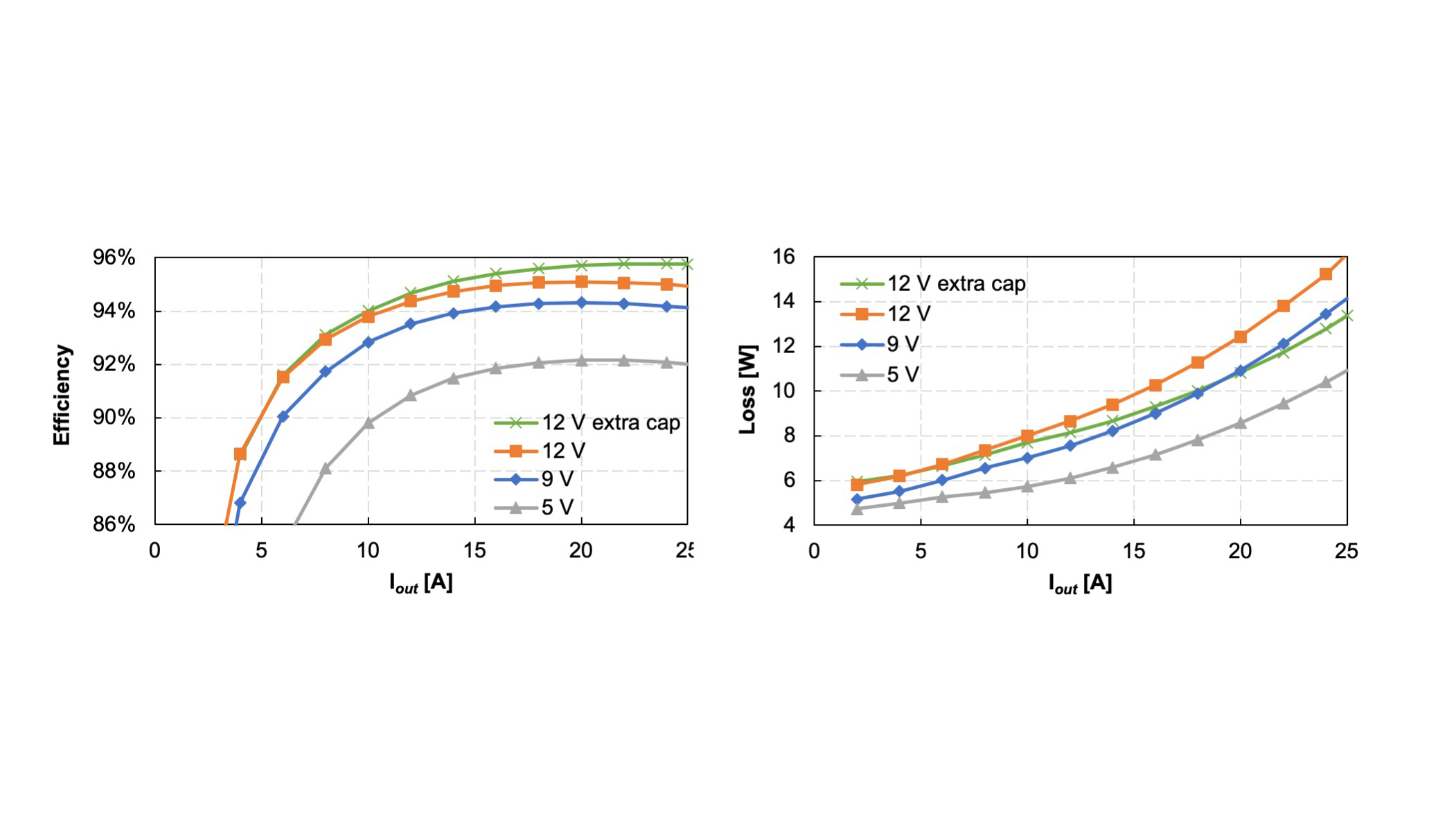 Figure 3: Measured efficiency and loss for the 1/16th brick converter
The test fixture has additional input capacitance of 47µF and additional output capacitance of 200µF. These extra capacitances help maintain controller stability. The fixture also provides programming ports and USB communication.
Design results
With 800 linear feet per minute (LFM) airflow, the measured thermal steady state efficiency and loss are shown in figure 3, for a range of output current up to 25A with different output voltages. The peak efficiency is 95% when the current is from 20 to 25A at 12V output. The maximum device temperature reached 100°C (see Figure 4).
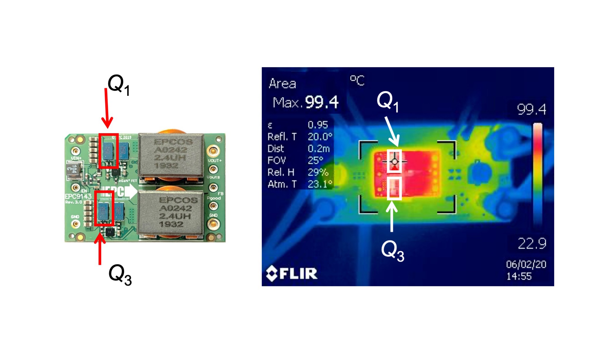 Figure 4: Thermal image of the 1/16th brick converter operating in thermal steady state
Due to space limitation, the brick converter can only fit a total of 8.2µF input capacitance. When an additional 2µF capacitance is added, the peak efficiency is improved to 95.8%, and the loss is reduced by 2.7W (15%).
The team from EPC and Microchip believes that these design criteria show that using GaN FETs could increase maximum load current in comparison with MOSFET designs.