


There is more data in the world today than ever before and there is one more thing you can be sure of – the levels of data that we store is only going to increase. Given the importance of this data to almost all aspects of our daily lives, highly secure data centres ensure that this data is never lost and always available for us when we need it.
With the high level of expectancy relating to data availability, data centres include significant amounts of redundancy. Yet, while this approach is necessary, it drives costs higher in a world where data storage is becoming a commodity and prices are falling.
Evolution
At the heart of delivering these high service levels is the uninterruptible power supply (UPS) that not only cleans and conditions the power, but also provides uptime capability during power outages.
The technology for data centre UPS is evolving and advances can deliver greater efficiency without sacrificing performance in UPS systems.
As data grows rapidly, scalability in modern data centres is an essential requirement to cover these storage demands. Power outages are becoming more frequent, meaning that UPS are an indispensable tool for delivering perfect data availability. It is, therefore, no surprise that research firm marketsandmarkets predicts that the market for UPS will reach $13.7 billion by 2022 and some markets, such as Asia-Pacific will continue to grow by around 7.2% annually.
There are three main types of UPS used today including offline, line interactive and online double conversion, these are offline, or standby power supplies, line interactive and offline double conversion power supplies.
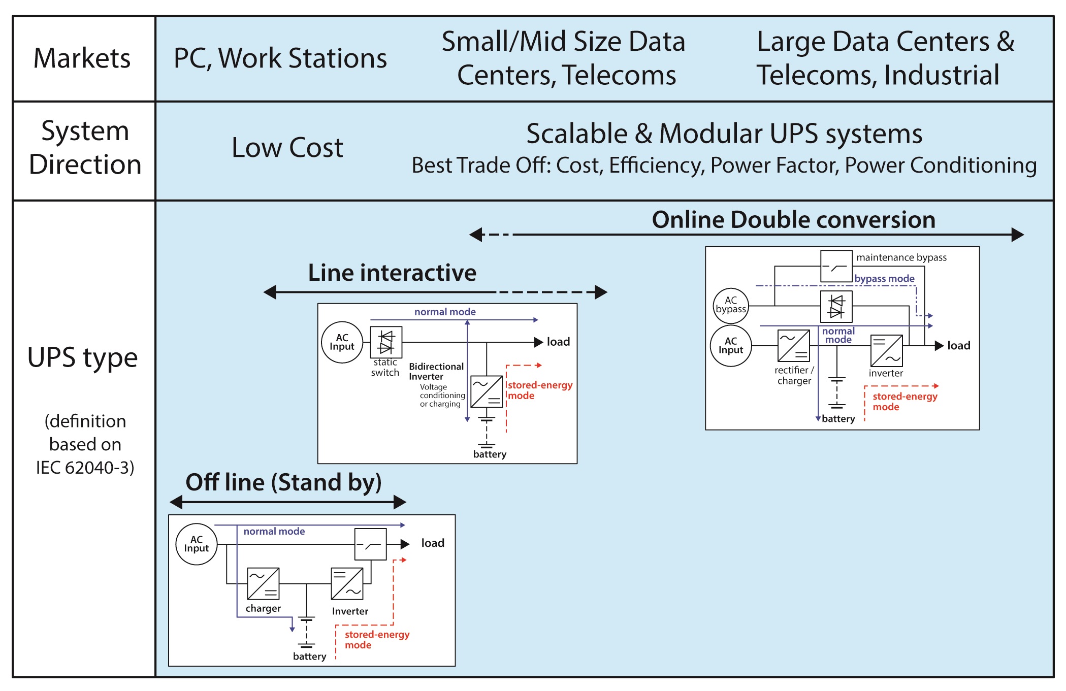
Figure 1: The three main UPS types in common use and their applications
While there are technical and performance differences, what all of these systems have in common is the need to be efficient, deliver power factor correction (PFC) at as close to unity as possible, and condition the provided voltage – while delivering all this at an ever decreasing cost.
Space challenges
The other factor that challenges designers is the space restrictions put upon them to achieve the requirements for the solution being developed. Space is at a premium in all data centres and operators are seeking to fill them with revenue-generating storage by every means possible, with the consequence that UPS systems are coming under increased pressure to be smaller. This has fuelled the popularity of rack type approaches based around modular UPS systems. The total power of each module is much less than that of the overall UPS system, so there is more flexibility for designers and a greater ability to scale solutions.
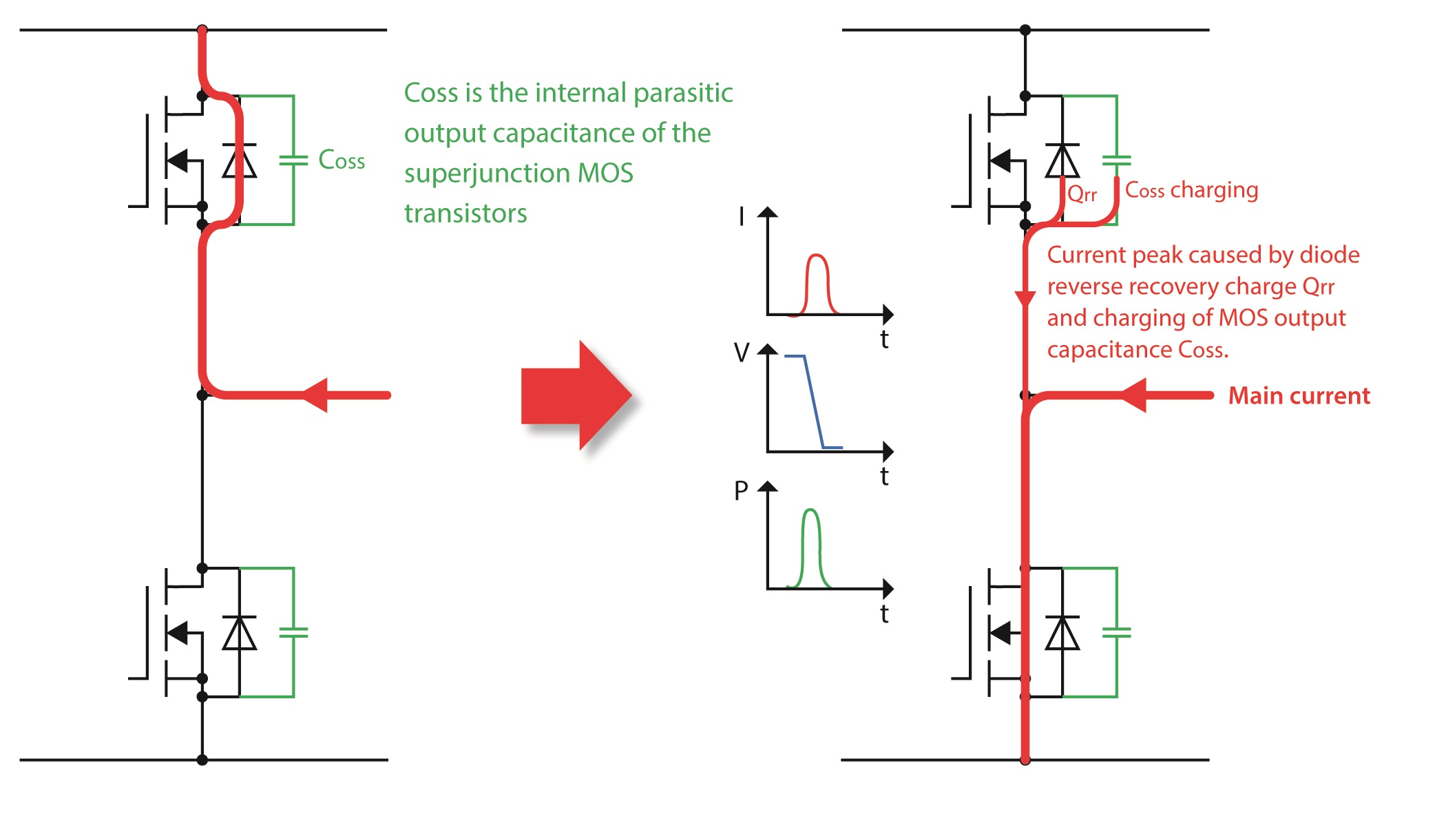 Figure 2: The half bridge topology has two primary switching loss mechanisms
Reducing the size of the UPS while maintaining power output (or sometimes increasing it) has a significant impact on power density. This challenge continues to get harder as smaller designs have less space for thermal management such as heatsinks. Active cooling with fans is often required, but these devices impact overall system efficiency as they also consume power.
While efficiency is probably the most important goal for operating cost management, power factor correction has a significant impact on cost as well. A poorly designed UPS can introduce undesirable voltage harmonics to the mains supply, which can have a negative impact on the operation of vitally important processing and storage equipment.
UPS performance improvement
A significant step forward in performance is expected once wide band gap gallium nitride (GaN) and silicon carbide (SiC) devices become fully available in quantity, with improved reliability and at a reasonable price level. Until then, designers are continuing to wring even modest performance improvements out of existing silicon-based MOSFETs.
Toshiba have patented a technique that is garnering a lot of attention as it allows existing silicon-based, superjunction MOSFETs to achieve performance levels approaching those of the forthcoming wide band gap solutions.
 Figure 3: Practical implementation of A-SRB
Based on ahalf-bridge topology, it can be demonstrated how the switching losses can become signficiant, while increasing the switching frequency. There are two primary aspects to these losses. The first is the reverse recovery charge (Qrr) stored in the freewheeling diode that causes a current peak in the lower transistor as it transitions into the conducting state. The second is the charging current peak during the reversal of the output capacitance (COSS) of the upper switching transistor.
Introducing A-SRB
Synchronous reverse blocking (SRB) is a technique that blocks the reverse current using a synchronously controlled transistor and channels the resulting reverse current through a SiC diode, thereby significantly reducing the impact of Qrr.
Toshiba has patented Advanced-SRB (A-SRB), a technique that negates the power losses from recharging the output capacitance (COSS) by pre-charging through increasing VDS to around 40V using a charge pump within the driver IC. This effectively reduces COSS by a factor of 100, and thereby significantly reducing the losses.
In a practical A-SRB realisation, the main switching transistor is a high-voltage superjunction DTMOS IV type MOSFET with a maximum blocking voltage around 650V. The series-connected blocking transistor is a low-voltage superjunction UMOS VIII type MOSFET with a blocking voltage of 60V. The freewheeling diode is a SiC Schottky diode as shown in Figure 3.
The T1HZ1F drive IC generates all necessary control signals from a simple PWM input signal and comprises of a patented solution that contains the control principle of the complete solution. This solution can be used in multiple applications where A-SRB has a benefit, including UPS, solar inverters, DC/DC converters and motor drive control. As A-SRB addresses the switching losses, higher switching frequencies can be used, allowing size and weight to be reduced in components such as the output filter without an efficiency penalty.
Topology comparisons
IGBTs are not as competitive since their switching frequencies are usually limited to around 20kHz. As an example, at an operating frequency of 50kHz and a load of 1kW, an inverter with an A-SRB topology would support an efficiency increase of 4%, when compared to a standard topology or IBGT solution. This permits a significant reduction in the thermal management requirements, reducing size, weight, complexity and cost of the system. In fact, in a data centre, the savings are higher overall as the reduction in heat generation additionally reduces the cost for air conditioning.
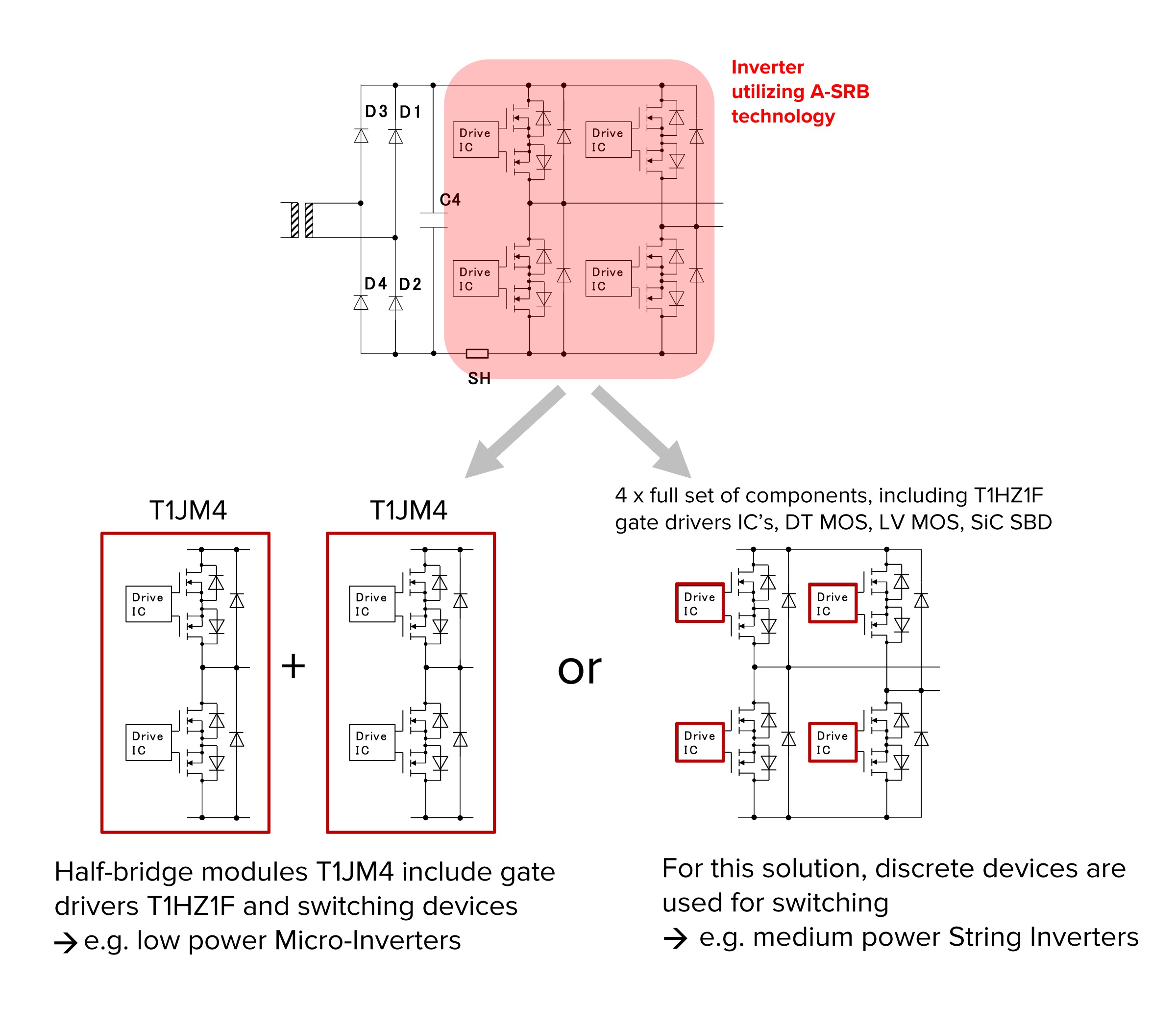 Figure 5: Discrete or modular solutions are chosen, based on required power level
To fully appreciate the advantages of A-SRB, both the increase in efficiency and the improved voltage conditioning need to be considered simultaneously.
Increasing switching frequency also helps to improve the generation of a high quality sine wave, however at 50kHz the switching losses increase sharply. Here A-SRB makes the most difference. At 50kHz it supports a significant improvement in voltage conditioning while still improving the efficiency. In systems without A-SRB, designers struggle to realize both improvements at the same time.
Modular and discrete A-SRB solutions
Several solutions are available to implement A-SRB functionality, depending upon the required power level. The T1JM4 module is a complete A-SRB solution for power levels up to 300W that integrates the gate drivers, switching transistors and SiC Schottky diodes.
If higher power levels are needed, Toshiba’s T1HZ1F gate driver can be used with discrete DTMOS, LVMOS and SiC SBDs for a scalable solution. The company offers the required components as complete kits of components
Toshiba’s patented A-SRB technique and associated drivers and modules provide a vital interim step, allowing designers to achieve performance levels today that are similar to those of wide band gap technologies.