


The demonstrated high-NA capability of the EUV interference lithography using this EUV source presents an important step for the AttoLab, a research facility initiated by imec and KMLabs to accelerate the development of the high-NA patterning ecosystem on 300mm wafers. The interference tool will be used to explore the fundamental dynamics of photoresist imaging and provide patterned 300mm wafers for process development before the first 0.55 high-NA EXE5000 prototype from ASML becomes available.
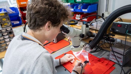
The high-NA exposure at 13.5nm was emulated with a coherent high-flux laser source of KMLabs in a Lloyd’s-Mirror-based interference setup for coupon experiments on imec’s spectroscopy beamline. This apparatus supplies critical learning for the next step, expansion to 300mm wafer interference exposures. In this arrangement, light reflected from a mirror interferes with light directly emitted by the 13.5nm laser source, generating a finely detailed interference pattern suited for resist imaging.
The pitch of the imaged resist pattern can be tuned by changing the angle between the interfering light beams. With this setup, 20nm line/spaces could for the first time at imec be successfully patterned in an Inpria metal-oxide resist (exposure dose range of ~54-64mJ/cm2, interference angle 20°) using a single-exposure, coated on coupon samples.
John Petersen, Principal Scientist at imec and SPIE Fellow, explained: “The high-flux laser source of KMLabs was used at a record small wavelength of 13.5nm, emitting a series of attosecond (10-18s) pulses that reaches the photoresist with a pulse duration that is a few femtoseconds (10-15s) in width. This imposed challenging requirements on the temporal coherence of the interfering waves.
“The demonstrated capability of this setup for emulating high-NA EUV lithography exposures is an important AttoLab milestone. It demonstrates that we can synchronise femtosecond wide pulses, that we have excellent vibration control, and excellent beam pointing stability. The 13.5nm femtosecond enveloped attosecond laser pulses allow us to study EUV photon absorption and ultrafast radiative processes that are subsequently induced in the photoresist material.
“For these studies, we will couple the beamline with spectroscopy techniques, such as time-resolved infrared and photoelectron spectroscopy, that we earlier installed within the laboratory facility. The fundamental learnings from this spectroscopy beamline will contribute to developing the lithographic materials required for the next-generation (i.e., 0.55 NA) EUV lithography scanners, before the first 0.55 EXE5000 proto-type becomes available.”
Next up, the learnings from this first proof of concept will now be transferred to a second, 300mm-wafer-compatible EUV interference lithography beamline that is currently under installation. This beamline is designed for screening various resist materials under high-NA conditions with a few seconds per single-exposure, and for supporting the development of optimised pattern, etch and metrology technologies viable for high-NA EUV lithography.
“The lab’s capabilities are instrumental for fundamental investigations to accelerate material development toward high NA EUV,” said Andrew Grenville, CEO of Inpria. “We are looking forward to deeper collaboration with the AttoLab”.
“Our interference tools are designed to go from 32nm pitch to an unprecedented 8nm pitch on 300 mm wafers, as well as smaller coupons,” added Petersen. “They will offer complementary insights in what is already gained from 0.33NA EUV lithography scanners – which are currently being pushed to their ultimate single-exposure resolution limits. In addition to patterning, many other materials research areas will benefit from this state-of-the-art AttoLab research facility. For example, the ultrafast analytic capability will accelerate materials development of the next-generation logic, memory, and quantum devices, and of the next-generation metrology and inspection techniques.”

