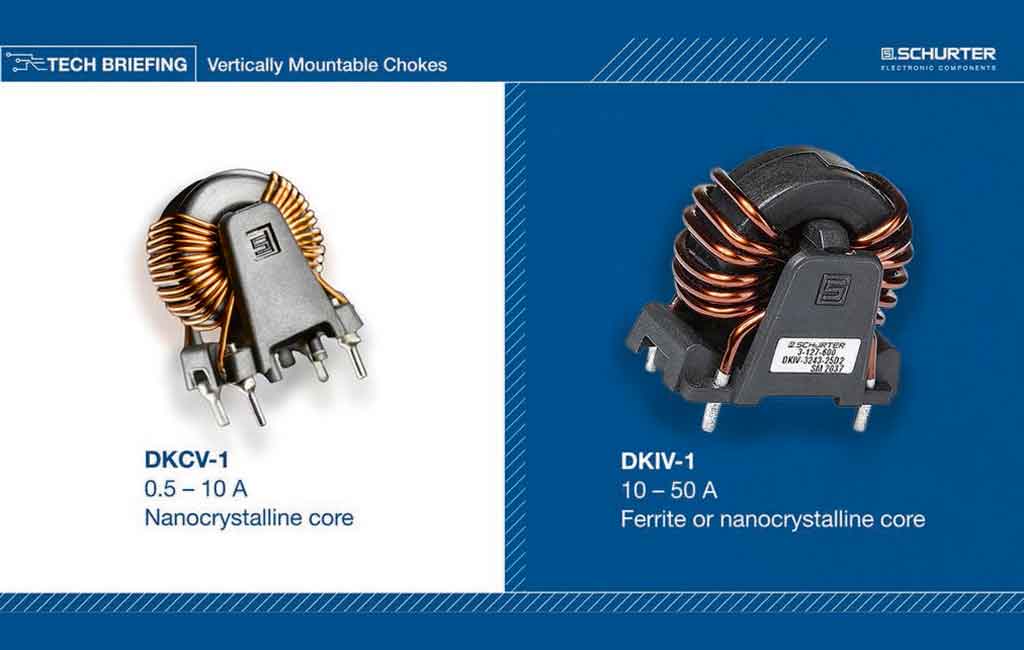


The semiconductor industry, the backbone of modern technology, continually pushes the boundaries of innovation to achieve higher performance, greater efficiency, and reduced costs. One of the most ground-breaking advancements in recent years is Extreme Ultraviolet (EUV) lithography.
As we look to the future, EUV technology is poised to play a crucial role in the evolution of semiconductor manufacturing, driving the next generation of microelectronics and sustaining Moore’s Law.
The state of EUV technology today
EUV lithography employs light with a wavelength of 13.5 nanometres, significantly shorter than the deep ultraviolet (DUV) light traditionally used in semiconductor fabrication. This shorter wavelength allows for the creation of much smaller features on semiconductor wafers, enabling the production of more densely packed and powerful microchips.
Currently, EUV technology is primarily utilised in the production of cutting-edge chips with feature sizes of 7 nanometres and below. Major semiconductor manufacturers like TSMC, Samsung, and Intel have integrated EUV lithography into their manufacturing processes, allowing for the continued scaling of transistors and enhancing the performance and efficiency of electronic devices.
“We believe that this EUV tech will enable us to introduce sub 5nm DRAM technology within the next hopefully 10 years. If we can achieve that, that will increase bit density of DRAM more than 3times.” Source: Samsung, Jinman Han, EVP Memory Sales and Marketing, Samsung Investor forum, November 2021
Challenges and innovations
Despite its advantages, EUV lithography faces several technical and economic challenges. These include the complexity of EUV light sources, the need for highly reflective mirrors, and the requirement for a vacuum environment to prevent absorption of the EUV light. Additionally, the cost of EUV equipment and the associated infrastructure is substantial.
Innovations in these areas are crucial for the widespread adoption of EUV technology. Advances in light source power and stability are essential for improving throughput and reducing manufacturing costs. Developments in mask technology and defect inspection methods are also critical to ensuring the reliability and yield of EUV-processed wafers.
Key terms making an impact on semiconductor scaling
EUV lithography is a crucial enabler for the continued scaling of semiconductors, often seen as the driving force behind Moore’s Law. By allowing for smaller feature sizes, EUV technology facilitates the creation of more powerful and energy-efficient microchips. This advancement propels progress in various fields, including artificial intelligence, 5G telecommunications, autonomous vehicles, and more.
To truly grasp these sophisticated technologies, it’s essential to understand key terminologies such as Depth of Focus (DOF), Resolution, Pitch, Optical Proximity Correction (OPC), Double Patterning, Critical Dimension (CD), and the Litho Gap. These terms are fundamental, much like the ABCs of constructing coherent sentences in English.
Let’s break down these concepts:
Depth of Focus (DOF): the range within which a feature remains in specification (CD, sidewall angle, resist loss) over a given range of exposure.
Resolution: the smallest feature that can be printed with a minimum depth of focus. There are two types of resolution in optical lithography: the smallest pitch (and half-pitch) and the smallest feature (critical dimension, CD).
The excitement around EUV stems from its capability to achieve the smallest pitch – an essential factor as smaller pitches enhance chip performance. Pitch resolution is influenced by the wavelength and numerical aperture (NA) of the lens used. The illumination wavelength refers to the light’s wavelength, while NA denotes the lens’s ability to focus this light.
To achieve reduced pitches, double patterning is employed in the semiconductor supply chain. This technique involves exposing a wafer twice with EUV light to achieve the desired tip-to-tip space.
Pitch: the distance between interconnect lines along an imaginary y-axis.
Tip-to-tip: the distance between interconnect lines along an imaginary x-axis.
Efforts in lithography have successfully reduced the pitch but have faced challenges in meeting customer requirements for tip-to-tip shrinkage, leading to what is known as the ‘litho gap’. Refer to the figure below to get an overview and differences.
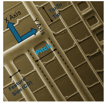
As semiconductor devices become more complex, the ability to integrate a greater number of transistors on a single chip becomes increasingly important. EUV lithography’s ability to produce finer patterns with high precision is essential for developing the next generation of processors, memory chips, and other critical components. The above illustration, generated using AI, aims to explain publicly available information about key terminologies such as pitch, resolution, feature size, and more to a general audience.
Future prospects and applications
Looking ahead, the future of EUV lithography is bright, with several exciting prospects and applications on the horizon:
High-NA EUV lithography: high-numerical aperture (NA) EUV systems are being developed to further improve resolution and enable even smaller feature sizes. These systems are expected to be critical for the production of 3 nanometre and sub-3 nanometre nodes.
Advanced packaging: EUV technology can enhance advanced packaging techniques, such as 3D stacking and heterogeneous integration. These approaches combine multiple chips into a single package, improving performance and reducing power consumption.
Quantum computing: the precise patterning capabilities of EUV lithography can be leveraged in the fabrication of quantum computing components, where ultra-small and highly controlled structures are required.
Photonic devices: EUV technology can also contribute to the development of photonic devices, which use light to transfer and process information. These devices have the potential to revolutionise data communication and processing.
Advancements in semiconductor tooling equipment research, such as Applied Materials’ Centura Sculpta and ASML’s EUV tools like the NXE 3400, play a crucial role in shaping the future of the semiconductor industry. These tools enable the development of faster, more efficient, and more powerful electronic devices that will transform our world.
EUV lithography represents a significant leap forward in semiconductor manufacturing technology. While challenges remain, ongoing innovations and investments are driving the maturation of EUV technology and expanding its capabilities. As EUV lithography continues to evolve, it will play a pivotal role in shaping the future of the semiconductor industry, enabling the development of faster, more efficient, and more powerful electronic devices that will transform our world.
The future of EUV is not just about maintaining the pace of Moore’s Law; it’s about breaking new ground and opening up possibilities that were once thought to be the realm of science fiction. As we stand on the brink of this new era, the advancements in EUV lithography promise to drive unprecedented progress in technology and innovation.
About the author:

Rupal Jain brings a wealth of experience in engineering, program management, and strategic alignment and stands as a distinguished person in the realm of semiconductor chip manufacturing. She has orchestrated projects spanning the entire spectrum from design conception to final delivery on a global scale, covering regions such as the USA, Asia, EMEA regions. Recognised for her profound expertise, Rupal is celebrated by prestigious certifications such as PMP, CSM, and Lean Six Sigma Black Belt. She holds a master’s in electrical and Electronics Engineering from NTU Singapore, in a joint degree program with TUM Germany. Her contributions have garnered international acclaim, earning her invitations to esteemed publications, media, jury, nominated memberships and coveted awards. Her books, “Mastering Project Management: PMP and Agile for Leaders’; ‘Semiconductor Essentials: A Leader’s Express Reference to Electronic Concepts’ and ‘Advancements in AI and IoT for Chip Manufacturing and Defect Prevention’, shares her valuable insights with the next generation of leaders and engineers.