


This results in successful work being somewhat at the mercy of trial and error approaches, making it time-consuming and laborious. The EU-funded ADOPSYS project has contributed to this shortcoming by developing new disruptive tools, including a new method for simulating and designing optical systems for both imaging and lighting systems.
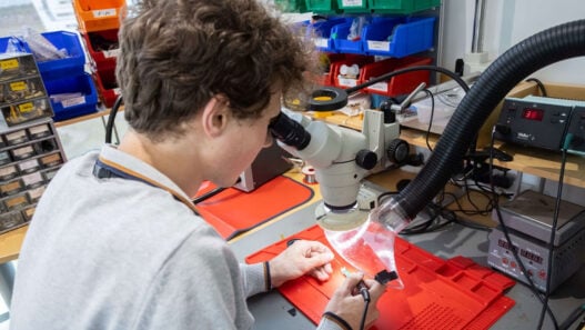
To sustain efforts, the project also facilitated specialist training, combining research with hands-on learning, for the next generation of highly skilled optical scientists.
Explaining the shortage of broad expertise for industrial optical systems modelling and design in Europe, Professor Paul Urbach, the ADOPSYS coordinator says, ‘Often the focus in universities is on newer topics such as nano-optics or meta-materials whilst optics, of more relevance to industry, is less addressed. This is especially true for optical design of lens and mirror systems for imaging and non-imaging applications.’
The ADOPSYS project employed computer modelling, with new computer programmes, drawing together a wider skill-set. This approach further developed the field tracing method to determine the light distribution in some planes after propagation through a non-paraxial optical system, that is where rays have widely differing propagation directions.
As a first, the project also took into account cascaded diffraction, which are the diffraction effects in multiple components of the system. The results were then benchmarked using existing tools, with some results also later experimentally verified.
The project also resulted in a series of five key design disruption tools. Firstly, ADOPSYS further improved the Simultaneous Multiple Surface (SMS) method for applications, to free form design of non-imaging systems such as collimators for automotive headlights and also extended the method for imaging systems such as high-end cameras.
Secondly, the project applied Saddle Point Construction (SPC) to locate viable optical systems from amongst pre-existing systems, by constructing saddle points from a given optimum design and then constructing at least two new optimal designs from every point.
Thirdly, ADOPSYS developed design methods for diffractive optical elements used under partially coherent illumination, such as Deep Ultra-Violet (DUV) and Extreme Ultraviolet (EUV) sources. These were based on a nonlinear iterative inversion algorithm.
As a fourth method, the project developed a computational method for free form construction in designs for lighting applications, in which the surface shape is found by solving a nonlinear integral equation.
Finally, optimal filters were designed that can be inserted into an optical imaging system, to enable image acquisition by computational post-processing. As Professor Urbach summarises, ‘Collectively, these design methods offer a toolkit which efficiently reduces the trial-and-error aspects of optical design efforts.’
In close collaboration with industrial partners there is a wide range of design problems to which ADOPSYS innovations can be applied, in particular energy efficient lighting systems, high-resolution imaging systems and machine vision, inspection and safety.
For example, SMS has been used to design 3D free forms RXI systems applied in automotive lighting because they are perfectly suited for the light patterns required for high and low headlamps.
Under the Marie-Curie Action funding, the investment that the project has made in transferable skills training for project team members, such as on Intellectual Property Rights (IPR), large projects collaboration and entrepreneurship, along with on-the-job industrial experience with industrial partners, has already started to bear fruit.
As Professor Urbach says, ‘Many of the Early Stage Researchers have built very successful, and ongoing, relations with European industries and indeed some of the ADOPSYS tools were developed in close collaboration with those industrial partners.’
Looking to the future Professor Urbach adds that, ‘In some cases, the new methods developed were not as fast as desired for their intended applications, so members of the ADOPSYS team will now be focussing on improvement in computational speed.’