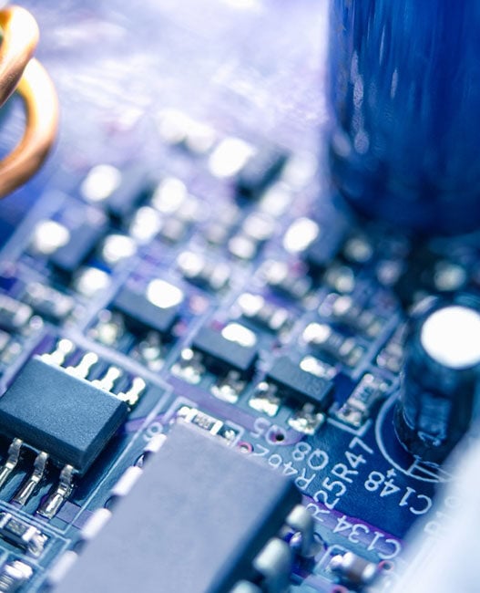


In recent times it has become apparent that traditional semiconductor packaging and copper interconnects can no longer meet the needs of today’s increasingly sophisticated devices. Electronic design engineers who are tasked with developing the next generation of AI and HPC (high performance computing) systems are dealing with a vast array of complex demands. Bandwidth, signal integrity, power consumption and thermal management are all at the forefront of their minds.
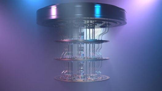
This is why photonic packaging and Co-Packaged Optics (CPO) are now under the spotlight. CPO is when optical fibres, used for data transmission, are integrated directly onto the same package or photonic IC die as semiconductor chips. The long copper trace between the switch and the optical module is changed to short, high-integrity connections between the ASIC and optical module. Advanced systems such as AI accelerators require compact, high-throughput packaging solutions.
Traditional semiconductor packaging vs photonic packaging & CPO
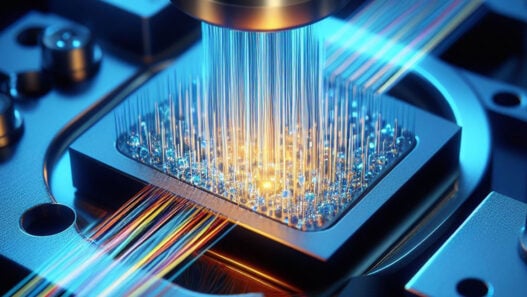
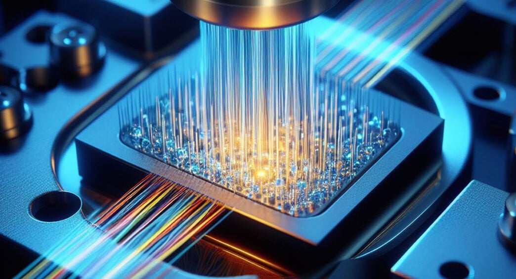
When the communication distance is more than 2 metres, traditional copper interconnects face increasing channel loss and power consumption at high data rates (for example, 112-Gb/s PAM4 and beyond), limiting practical reach and driving the need for advanced equalisation or shorter electrical links. Using optical interconnects can support multi-terabit-per-second data rates over long distances with only slight signal loss, while enabling much higher I/O bandwidth density, significantly expanding the I/O capacity per chip. Optical signals are also resistant to electromagnetic interference (EMI) and crosstalk, so components can be integrated more tightly without impacting on signal integrity.
Electrical signalling at high data rates often leads to power consumption and heat concerns. However, with optical signalling, energy per bit can be drastically cut and thermal management is better. This means that design engineers can balance their power budgets, which can be especially challenging with AI/ML and data centre designs where I/O power is a key factor.
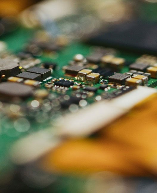
CPO & photonic package design
Photonic integration technologies allow for the miniaturisation of transceivers and enable CPO or on-package optical I/O. This approach is unlocking new opportunities for novel advanced architectures, including chiplet-based systems and heterogeneous integration, which are fundamental for scaling AI systems for the future. However, there are issues with CPO that must be addressed and this is why photonic package design is proving to be so important.
Although CPO shortens high-speed electrical links and improves channel integrity, careful package design is still required to manage parasitics, RF coupling, and power delivery noise. Effective thermal management and thermal design are also essential to ensure system reliability. Integrating photonics with electronics may require thermoelectric coolers (TECs) and heat sinks, as well as thermal simulations, but many data centre CPO approaches aim to avoid TECs due to their power overhead.
Optical misalignment can mean that there are substantial insertion losses that may negatively impact on performance. Sub-micron alignment is a tricky technical undertaking. Passive alignment techniques with etched features or alignment markers are cost-effective, but can be less accurate. Active alignment, such as using real-time optical feedback, offers the advantages of improved performance and efficiency, but increases the cost and complexity considerably. In terms of testing, this can be complicated with optical components, but can be managed by using built-in test waveguides, automated optical probing systems and standardised test procedures.
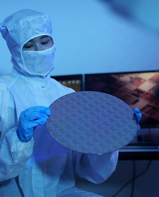
Advanced photonic package design
Typically, companies operating in this sector concentrate on either packaging or photonics. Sarcina Technology are experts in semiconductor packaging, electrical engineering, and photonics, removing the need to have separate electrical and optical packaging specialists. Sarcina provides an extensive selection of advanced photonic package design services for customers innovating in the AI, HPC, and networking space.
Sarcina offers expertise in CPO design, silicon photonics package integration, optical I/O and interposer design, photonic substrate design, custom optical connector and fibre attach, as well as thermal and mechanical co-design. Whatever an electronic design engineer is working on – whether it’s a co-packaged optical engine or a photonic AI accelerator – the Sarcina team is focused on ensuring seamless and fast integration, reducing the time-to-market.
Advanced photonic package design looks likely to play a really important role in the future of high-performance electronics, enabling the challenges with CPO and photonic packaging to be overcome, and exciting new architectures to be delivered that would not be achievable with traditional semiconductor packaging alone.
About the author:

Dr. Larry Zu, CEO at Sarcina Technology