7 steps to a successful analogue ASIC

This paper is an educational piece directed toward engineers, engineering managers and corporate decision makers who are seeking new ways to shrink the size and lower the cost of their products as well as protect their IP through custom integration. By Bob Frostholm, Vice President of Marketing & Sales, JVD Semiconductors.

This simple guide will help them understand all the many pieces involved in committing to an analogue ASIC semiconductor and hopefully to eliminate their preconceived fears about engaging with ASIC semiconductor companies.

The paper addresses the following key points:
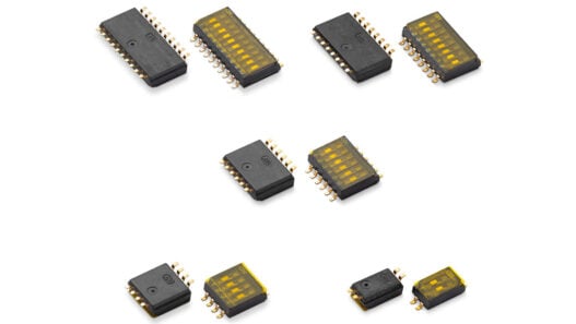
  • Bill of materials;
  • Resource planning;
  • Project longevity;
  • Project anticipated volumes;
  • Risks;
  • NRE & tooling; and
  • Production.

Read and download the full whitepaper below.

Keep Up to Date with the Most Important News

By pressing the Subscribe button, you confirm that you have read and are agreeing to our Privacy Policy and Terms of Use
Previous Post

Bluetooth low energy front-end modules operate up to 2.485GHz

Next Post

Open frame AC/DC power supply offers 400W at 92% efficiency