


This article originally appeared in the April ’22 magazine issue of Electronic Specifier Design – see ES’s Magazine Archives for more featured publications.
Due to its nature of switching large currents, an SMPS generates a fair amount of noise. SMPS topology can influence filter design, for example, a dual interleaved boost topology creates less noise than a simple boost converter.
Very often, a high switching frequency converter is chosen for a compact design but high switching frequency can be a cause of excessive EMI. While wide-bandgap devices based on SiC or GaN are popular in power converter designs to increase efficiency, the fast switching elements accentuate noise generation. It is therefore helpful to minimise the parasitic elements in the whole design, including the PCB. For example, the high voltage switching element combined with a connection to a metal housing for cooling will create a parasitic capacitance, which can act as a path for common mode noise to exit the system.
EMI input filter structure
An EMI input filter typically consists of two functional parts, one to suppress common mode noise, the other part to suppress differential mode noise.
For an AC/DC converter, the key components for the differential mode EMI filter are the differential mode inductors and the X-capacitors. For the common mode EMI filter part they are the common mode choke and the Y-capacitor. In some cases, the differential mode inductors can be omitted as the common mode choke can also act as differential mode inductor.
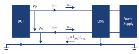
Figure 1. Common mode / differential mode flow
Separating noise
The EMC standard requires that the conducted emissions on both power lines are measured and that the voltages are below the specified limit at every frequency in the range. This measurement is performed sequentially on power lines. This is sufficient to pass the conducted emission test standard but does not provide any insights into the noise propagation mechanisms. The principle of how the noise current flows within the system is shown in Figure 1.
The common mode current portion Icm flows from the device under test (DUT) on both lines into the LISN (line impedance stabilisation network) and to the DUT via the external ground path, resulting in the sum of the two current portions in the external ground path. The amplitude and phase are the same on both conductors, positive and negative. The differential mode current shows a different characteristic. Here, the current on the positive conductor flows into the LISN, the return path of the noise is the negative conductor. The only difference is the phase, the two currents differ by 180° – ideally they should each other cancel out.

Figure 2. Enhanced measurement setup using dual-output LISN
To separate the common mode and differential mode noise terms:
IP = ICMa + IDM and IN = ICMb – IDM can be used to calculate the voltages on the two conductors:
VP = (ICMa + IDM) * ZLISN
VN = (ICMb − IDM) * ZLISN
Based on the relations between individual voltages and common mode and differential mode voltages (VP + VN = VCMa + VCMb) the common mode and differential mode voltages can be calculated as: VCM = VP + VN and VDM = ½ (VP – VN).
The common mode value is twice the differential mode noise level, or 6dB extra, which has to taken into consideration when evaluating the results.
The calculation works best, if the setup (e.g., cable, components of the LISN) is as symmetrical as possible as the noise on the two conductors must be measured at the same time.
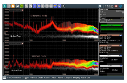
Figure 3. A reference level measurement with no EMI filter
A simple but effective setup to separate common mode and differential mode noise uses a dual-output LISN (or two identical LISNs) to probe on both power lines. The signals are captured by two channels of an oscilloscope (Figure 2). The sum and difference signals are calculated on the oscilloscope as well as the fast Fourier transformation (FFT). This gives direct access to the common mode and differential mode noise signals.
This method provides reasonably accurate results, although any non-symmetry between the two LISNs will influence the measurement. The same cable lengths must be used and they must be sufficient quality to avoid shift in time or loss in amplitude, which would affect the ability to separate the noise components.
An oscilloscope with a low-noise front end, direct input of frequency parameters, or resolution bandwidth, and a sufficiently fast FFT function should be used.
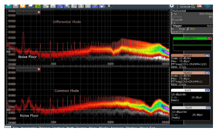
Figure 4. Reference level measurement with the differential mode filter applied
Case study
This example uses a step down buck converter and a PI-LC filter for damping differential mode noise. No common mode filters are included on the PCB, so a common mode choke is attached externally. The converter has no housing, so the PCB is placed on an isolation block on a metal ground plane. This setup avoids generating excessive common mode noise.
The first measurement (shown in Figure 3) shows the highest spectrum in the input power conductors. A reference level measurement has established the noise level of the system while the DUT is switched off. The extra 6dB in differential mode was compensated by dividing the sum expression by two before performing the FFT. For common mode, the sum expression is used directly as the total amount of common mode noise is represented by the sum of the two measurement channels.
The peak at 300kHz in the reference line is caused by the system, not the converter, and can be ignored, at least up to 25dBµV. The high magnitude differential mode noise (approximately 65dBµV) during the measurement at 300kHz is caused by the switching frequency of the converter. The harmonic and all higher odd multiples of this frequency are caused by the reflected ripple current, which dominates the differential mode spectrum. In the common mode spectrum, some peaks are also visible.
An LC filter is calculated to damp the fundamental magnitude at 300kHz. The calculated filter resonance frequency is 19.3kHz, which should result in a suppression of about 40dB at the switching frequency. The filter structure is second order and thus the damping is about 40dB/decade.
In Figure 4, the differential mode noise is reduced by up to 10MHz, damped up to 30dB compared to the unfiltered value. In the higher frequencies, the filter is not as effective – noise is only damped by up to 10dB.
To damp the common mode noise, an additional filter is added. This example used a common mode choke from Würth Electronic (Figure 5).
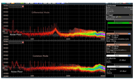
Figure 5. The common mode choke efficiently dampened common mode noise
Common mode noise is reduced from 2MHz to 60MHz and differential mode noise is also damped. (Leakage inductance from the common mode choke functions as a differential filter.) Differential mode noise may also be affected by the absence of a PCB for the common mode choke, meaning some asymmetrical components may contribute to the damping effect.