

Consumer demand is driving the need for ever-faster silicon chips, also known as integrated circuits (ICs) or semiconductors. In tandem with the trend for increasingly compact electronic devices, there is a distinctly unwanted side effect: heat. The faster an IC runs, particularly in a small space, the hotter it gets. Electronics need to operate within a specified temperature range to achieve optimal operation, so the need to remove heat from an IC and disperse it effectively and safely is very real. The answer? Adopting the latest generation of appropriately specified and applied thermal interface materials.
Any OEM or CEM electronics companies operating in sectors such as telecommunications, information technology, power conversion, medical device, defence, or transportation will know all about the thermal challenges associated with faster ICs. It seems every new generation of an electronic product requires higher power in a smaller package, exacerbating the need for optimal thermal management.
The good news for these companies is the relentless innovation drive at thermal management solutions suppliers such as Parker Chomerics. Developing high-performance products is the only way to meet the thermal and design challenges of tomorrow’s systems. Drivers of new thermal interface materials (TIMs) include lower thermal impedance, higher thermal conductivity, better conformability, increased reliability, greater adhesion and longer service life, as well as easier handling, application and use.
Chip cooling
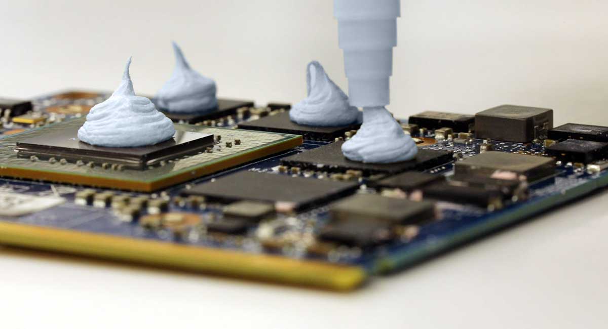
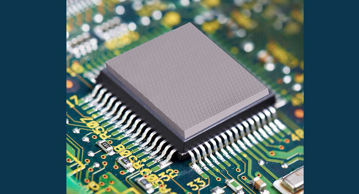
Applying a TIM to an IC surface requires intimate contact between two surfaces. Even though the surface electronic components and heatsinks may appear flat to the naked eye, their characterisation typically involves some level of microscopic surface roughness and non-planarity. In practice, this means surfaces feature some degree of concave, convex or twisted shape. Contact between these surfaces would only occur at the surface high points, with the low points forming air-filled voids or interstitial air gaps that resist heat dissipation due to the insulative properties of air.
The way to eradicate these air gaps from the interface is to adopt gap-filling thermally conductive TIMs that conform to the irregularities of the surfaces, such as dispensable gels and pads. As a TIM of this type offers greater thermal conductivity than the air it replaces, resistance across the joint reduces, as does the component junction temperature.
As well as providing essential thermal properties such as thermal impedance, thermal conductivity, co-efficient of thermal expansion and heat capacity (ability of the material to store heat), TIMs also offer electrical properties like voltage breakdown and volume resistivity. This is in addition to physical or elastomeric properties, such as vibration dampening.
A variety of material types are available, mostly developed in response to the changing needs of electronics industry applications. Among the most common materials for electronic components such as latest-generation high-speed ICs are dispensable gels and pads.
Thermally conductive gels, like the THERM-A-GAP GEL range from Parker Chomerics, are single-component dispensable thermal gap fillers that require no curing and prove highly suitable for dispensing over an electronic component such as an IC for effective cooling. Conforming perfectly to the surfaces of the heat-generating and heat-dissipating surface, thermal gels have the potential to eliminate multiple thermal gap filler pad part sizes, while their cross-linked gel structure provides superior long-term thermal stability and performance. Gels are often preferable for filling complex shapes or providing additional adhesion.
Thermally conductive pads, like the THERM-GAP PAD series from Parker Chomerics, come into their own for certain applications. These soft, silicone and non-silicone elastomers are ideal where heat must be conducted over a large and variant gap between an IC and a heat dissipating surface such as a heatsink. Pads are popular for applications requiring frequent maintenance or replacement, or in mass production scenarios prioritising consistency and convenience. These products also help in mechanical stability by absorbing shock and vibration.
Board level shielding
Of course, chip cooling is only half the battle when looking to provide ICs with the protection they need for optimal performance and safety. The other major threat is electromagnetic interference (EMI), essentially any type of interference caused by electromagnetic fields that can disrupt the signal and operation of an electronic device.
EMI, either incidental or malicious, can lead to the malfunction or even failure of electronic components such as ICs. Effective shielding is therefore of paramount importance, particularly in safety-critical electronics applications such as those prevalent in sectors such as aerospace, defence, power generation, automotive/e-mobility, and healthcare.
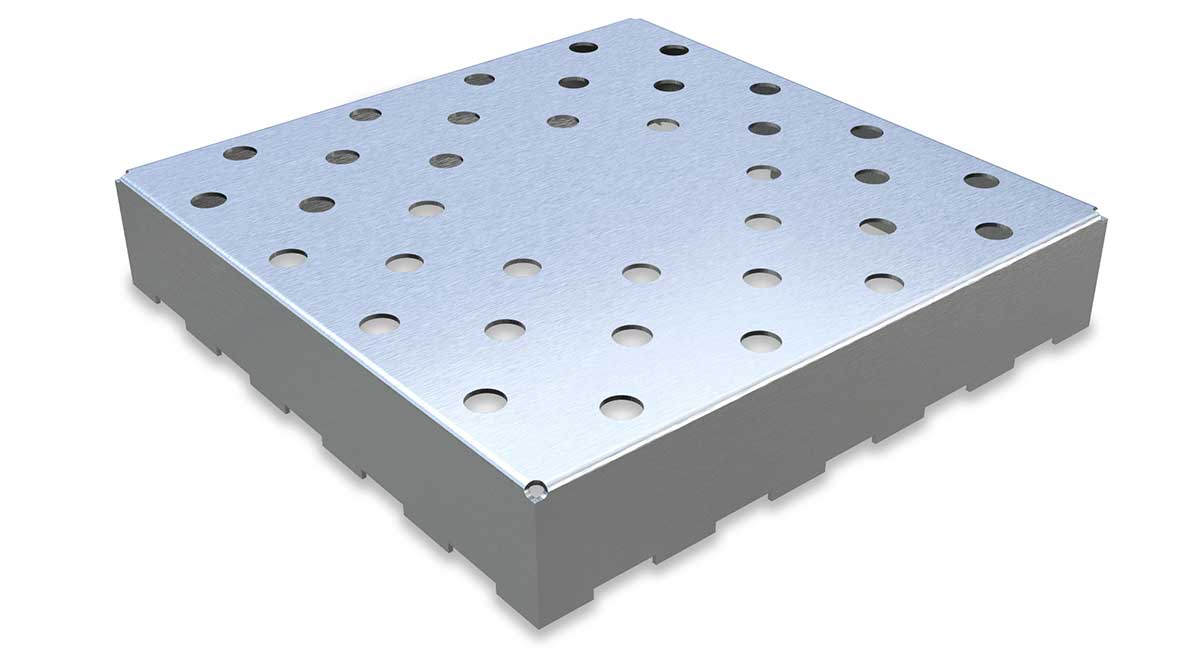
Board-level shielding and stamped metal components are the optimal solution for reducing or limiting the effects of EMI. Solutions of this type help isolate board-level components, minimise crosstalk and reduce susceptibility to EMI by forming an electrically conductive ‘box’ or faraday cage around the components.
Component design options include one-piece, two-piece and multi-cavity configurations, while also incorporating precise mounting methods such as surface mount technology (SMT). The manufacture of EMI shielding components is typically via a stamping/forming or drawing process based on specific design criteria and end-user requirements. Board level shields can also integrate unique design features including, but not limited to, ventilation holes, complex geometries, embossing and orientation markings.
Parker Chomerics offers board-level shielding products in several base materials and plating options, including tin-plated cold-rolled steel, nickel-silver, aluminium and stainless steel, with other materials and plating options are available on request.
Component integration
As each application is unique, board-level shields must not only offer excellent high-frequency EMI shielding, but also high customisation potential and suitability for seamless integration into full PCB builds. By working with a reputable supplier such as Parker Chomerics it is possible to simplify assembly and reduce supply chain and logistics concerns. Examples of integration include thermal interface products, RF-absorbing coatings, electrical grounding materials and heatsinks.
A critical step in the design process is identifying a suitable technology partner experienced in both EMI and thermal interface material development: one that can deliver expert application and engineering support, EMI emissions testing, and the fast and cost-effective prototyping of board-level shielding components.
Thermal management and EMI interference are long-standing pain points for electronics engineers. However, with the right specification and application, the latest advances in TIMs and board-level shields mean both OEMs and end users can have confidence in optimally performing electronic components.

This article originally appeared in the November’25 magazine issue of Electronic Specifier Design – see ES’s Magazine Archives for more featured publications.