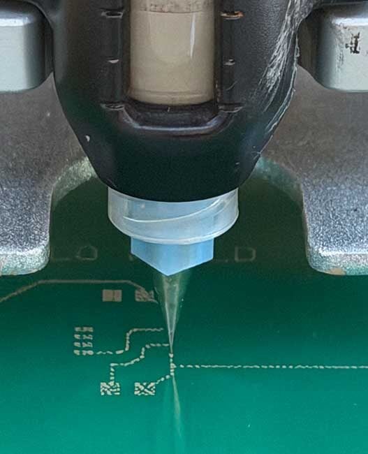
This project will combine the expertise of the project partners with Infinitesima’s Rapid Probe Microscope (RPM) technology, enabling in-depth three-dimensional (3D) surface detection, high-speed imaging, and interferometric accuracy. This will address the industry’s urgent need for detailed 3D metrology information throughout the full structure of features at high throughput and in high-volume manufacturing environments.
As part of this project, Infinitesima will be siting a tool at imec, a research and innovation hub in nanoelectronics and digital technologies. The system will be used to advance next-generation device development by partners including ASML to continue with the characterisation and development of high- NA EUV resist imaging. Infinitesima will work closely with imec to develop new tool capabilities and enhancements. This joint effort aims to deliver true 3D process control – critical for enabling the production of future semiconductor devices.
Infinitesima’s partnership with imec began in 2021, starting with enabling tip-induced nanoscale tomographic sensing using its patented RPM for research and failure analysis applications. This new collaboration marks the expansion of the Infinitesima-imec partnership into high-speed, in-line production metrology, supporting the semiconductor industry’s advancing inspection and metrology demands for sub-nanometre features and increasingly complex 3D structures.
“We are delighted to extend our existing collaboration with imec to support the critical metrology challenges of some of the most critical process steps for next generation semiconductor processes,” said Peter Jenkins, CEO of Infinitesima.
With this expanded partnership, Infinitesima is set to reinforce its leading position in in-line semiconductor metrology, supporting the industry’s evolution toward smaller and increasingly complex device architectures.


