


This article originally appeared in the May’22 magazine issue of Electronic Specifier Design – see ES’s Magazine Archives for more featured publications.
With the high integration and high efficiency revolution in motor/inverter systems, SiC and GaN FETs are beginning to replace MOSFET and IGBT due to their smaller size, higher switching frequency, and lower heatsink advantages. However, high CMTI capability is required for the isolation components. Higher accuracy current measurement is also needed. The next-generation isolated modulator greatly increases the CMTI capability and improves the accuracy itself. By Nandin Xu, Product Applications Engineer, Analog Devices
What is common-mode transient immunity?
Common-mode transient immunity specifies the rate of the rise and fall of a transient pulse applied across the isolation boundary, beyond which clock or data is corrupted. Both the rate of change and the absolute common-mode voltage (VCM) of the pulse are recorded
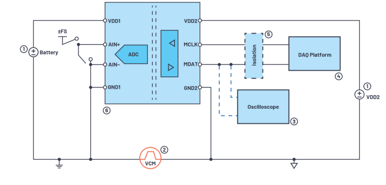
The new isolation modulators are tested under both static and dynamic CMTI conditions. Static testing detects single-bit errors from the device. Dynamic testing monitors the filtered data output for variations in noise performance to a randomised application of the CMTI pulse. A detailed test block diagram is shown in Figure 1.
CMTI is important because high slew rate (high frequency) transients can corrupt data transmission across the isolation barrier. Understanding and measuring the susceptibility to these transients is critical. ADI’s test methods are based on the IEC 60747-17 standard, which involves measuring methods of common-mode transient immunity (CMTI) for magnetic couplers.
 How to characterise the CMTI for an isolated modulator on the bench
The simplified CMTI test platform includes the following items shown in Figure 1:
- A battery power supply for VDD1/VDD2 • A high common voltage pulse generator
- An oscilloscope used to monitor data
- A data acquisition platform used to analyse the data and a 256 decimation sinc3 filter used for an isolated modulator
- An isolation module (normally optical isolation is used)
- An isolated modulator
For the static and dynamic CMTI test, the same platform is used – only the input signals are different. This platform also can be used to test other isolated products’ CMTI performance.
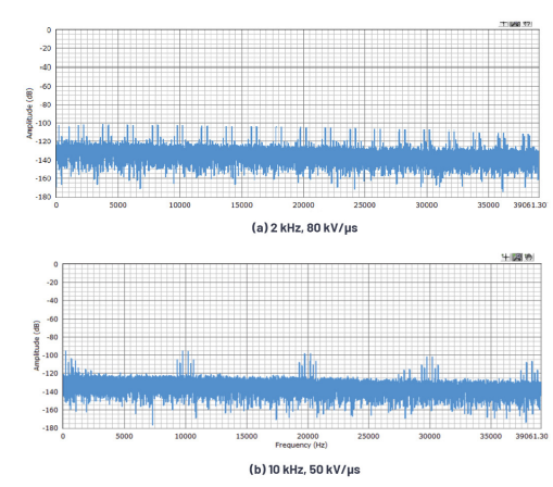
For isolated modulators, the one-bit stream data will be decimated and filtered, then transferred to the control loop in the motor control system, so the dynamic CMTI test performance will be more comprehensive and useful. Figure 2 and Figure 3 show the time and frequency domain CMTI dynamic test performance under different CMTI levels.
From Figure 2 we can see that the spur will become larger when adding the higher VCM transient signal for the same isolated modulator. When the VCM transient signal is over the isolated modulator specification, a very large spur will appear in the time domain (as noted by Figure 2c). This has serious consequences when using in the motor control system, resulting in a large torque ripple.
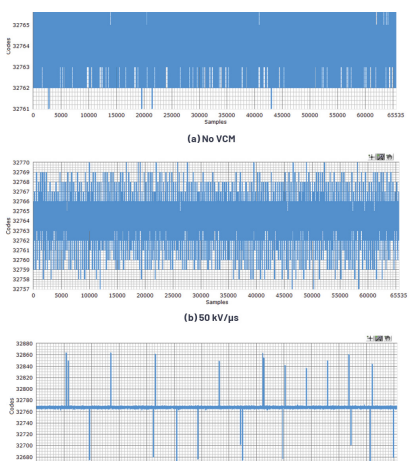
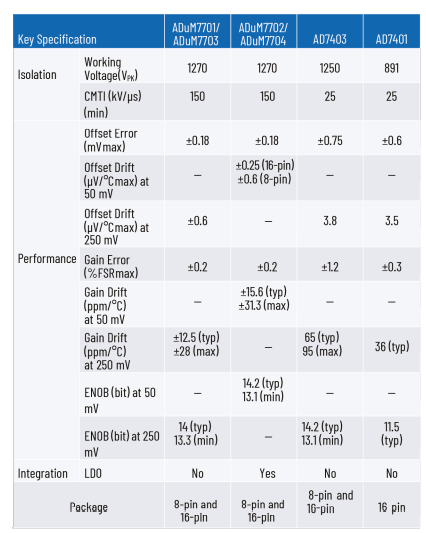
Figure 3 shows the FFT domain performance under different frequency transients (which means keeping the VCM transient level by changing the period of the transient). The results in Figure 3 show that the harmonic is highly relative to the transient frequency. Thus, the higher the CMTI capability of the isolation modulator, the lower the noise level in the FFT analysis. Compared with previous generation isolated modulators, the next generation of ADuM770x devices increases the CMTI capability from 25 kV/µs to 150 kV/µs, which highly improves the system transient immunity, as detailed in the comparison data in Table 1.
 System-level compensation and calibration
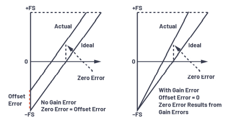
In a motor control or inverter system, the higher the accuracy of the current data, the more stable and efficient the system. Offset and gain error are common sources of DC error in ADCs. Figure 4 shows how offset and gain error affect the ADC transfer function. These errors can contribute to the system as torque ripple or speed ripple. To limit the error impact for most systems, these errors can be calibrated out at ambient temperature.
Otherwise the offset drift and the gain errors over the complete temperature range are a concern, as they are more difficult to compensate. Provided that the system temperature is known, compensating for offset and gain error drift is achievable (although costly and time consuming) for converters with linear and predictable drift profiles by adding a compensation factor to the profile to make the offset drift profile as flat as possible. This detailed compensation method is described in the application note AN-1377. This method can reduce the drift figure specified in the AD7403/AD7405 data sheets by up to 30% for offset drift and 90% for gain error drift, and it can be applied to any other converter components when you want to improve the offset and gain error drift at the system level.
How to use the chopping technique
Alternatively, a design called the chopping technique is more efficient and convenient for a system designer to use, and the chopping function can also be well integrated with the silicon itself to minimise offset and gain error drift. The chopping scheme is shown in Figure 5, where the solution implemented on an ADC is to chop the entire analog signal chain to remove any offset and low frequency errors.
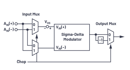
The differential input to the modulator is alternately inverted (or chopped) at the input multiplexer, and an ADC conversion is performed for each phase of chop (switch the mux to the “0” or “1” state). The modulator chopping is reversed in the output multiplexer before passing the output signal to the digital filter.
If the offset in the sigma-delta modulator is represented as VOS, then the output is (AIN(+) − AIN(−)) + VOS when chop is 0 and the output is −[(AIN(−) − AIN(+)) + VOS] when the chop is 1. The error voltage, VOS, is removed by averaging these two results in the digital filter giving (AIN (+) − AIN (−)), which equals the differential input voltage without any offset term.
AIN(−)) + VOS when chop is 0 and the output is −[(AIN(−) − AIN(+)) + VOS] when the chop is 1. The error voltage, VOS, is removed by averaging these two results in the digital filter giving (AIN (+) − AIN (−)), which equals the differential input voltage without any offset term.
Recomemended circuit and layout design
The typical current measurement circuit of a motor system is shown in Figure 6. While there are three phase current measurement circuits required in the system, only one is shown in the block diagram. The other two phase current measurement circuits are similar and represented by the blue dotted line.
From the phase current measurement circuit, we can see that one side of the RSHUNT resistor is connected to the input of the ADuM770x-8. The other side is connected to the high voltage FETs (these can be IGBT or MOSFET) and the motor.
The overvoltage, undervoltage, or other voltage instability conditions always occur when the high voltage FETs change the status. Correspondingly, the voltage fluctuation of the RSHUNT resistor will pass to the ADuM770x-8 and the related data will be received on the DATA pin.
The layout and system isolation design can improve or degrade voltage instability conditions, which affects phase current measurement accuracy.
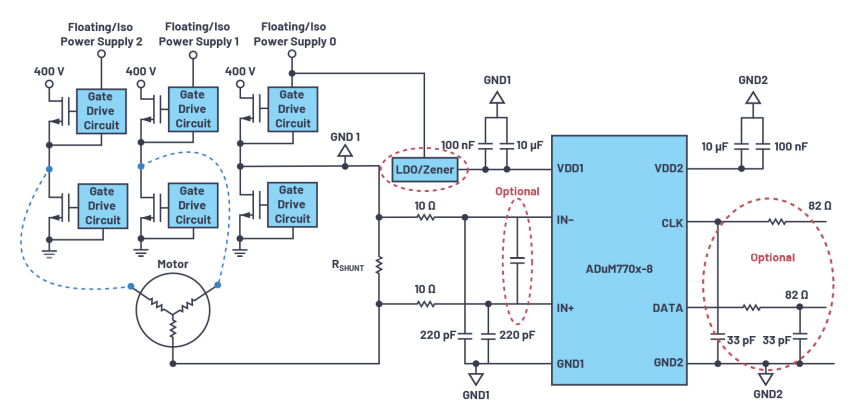
The recommended circuit setup as shown in Figure 6 is:
- For VDD1/VDD2 decoupling, 10 µF/100 nF caps are needed and should be placed as close as possible to the corresponding pins
- A 10 Ω/220 pF RC filter is needed
- An optional differential capacitor is recommended to reduce the noise effects from the shunt. Place the capacitor close to the IN+/ IN– pin (a 0603 package is recommended)
- An 82 Ω/33 pF RC filter is recommended when the digital output line is long. For good performance, a shielded twisted pair cable should be considered
- For higher performance requirements, consider using a 4-terminal shunt resistor
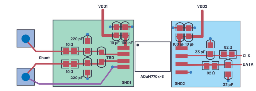
To reach the best performance, a good layout is also necessary. The recommended layout is shown in Figure 7. Differential pair routing from the shunt resistor to the IN+/IN– input pins is recommended to enhance the common-mode rejection capability. The 10 Ω/220 pF filter should be placed as close as possible to the IN+/ IN– input pins. The 10 µF/100 nF decoupling capacitors should be placed close to the VDD1/ VDD2 power supply pins. It’s recommended that the partial ground plane GND1 be placed under the input related circuit to improve the signal stability. The independent GND1 line (shown in purple and paralleled with the differential pair routing line), star connection from the shunt resistor to ADuM770x-8 GND pin is needed to decrease the power supply current fluctuation effect.
Conclusion
The latest ADuM770x isolated sigma-delta modulators increase CMTI to the 150 kV/µs level and improve temperature drift performance, which highly benefits current measurement applications. Using the recommended circuit and layout will be helpful during the design stage.
References
ADuM7704 data sheet. Analog Devices, Inc., August 2020.
Heo, Hong-Jun; Seon-Ik Hwang; Jang-Mok Kim; and Jin-Woo Choi. “Compensating of Common Scaling Current-Measurement Error for Permanent Magnet Synchronous Motor Drives.” 2016 IEEE 8th International Power Electronics and Motion Control Conference (IPEMC-ECCE Asia), May 2016.
McCarthy, Mary. “AN-1131: Chopping on the AD7190, AD7192, AD7193, AD7194, and AD7195.” Analog Devices, Inc., October 2011.
Merino, Miguel Usach and Gerard Mora Puchalt. “Integrated Capacitive PGAs in ADCs: Redefining Performance.” Analog Dialogue, Vol. 50, No. 3, August 2016.
O’Byrne, Nicola. “MS-2652: Measurement Techniques for Industrial Motion Control.” Analog Devices, Inc., June 2014.