


As digitalization increases, so does the demand for new sensor technologies. Smart systems are revolutionizing the communication between applications and their users. First of all, a balance between more and more complex sensor networks with data processing and simpler, more user friendly operator support is necessary. The trend toward miniaturization makes it difficult to equip parts having only a limited amount of space with conventional sensors. The binder ITC has, for this reason, developed a new direct printing technique – the binder method – that can overcome all these challenges. According to Dr. Stefan Ernst, one of the co-developers of the new printing technique, the advantages are obvious. “The printed electronics need less space. In addition, they are more flexible in application and more cost efficient.“
The area of printed electronics has been a research topic for binder since 2009. In 2016, the newly founded Innovation & Technology Center started operation. With the help of a recently developed transfer printing technique, binder was able, for the first time, to apply planar functional electronic layers with a thickness of maximum precision to textured, three-dimensional surfaces in only one printing pass. In this way, circuit traces, sensors and displays, for example, can be printed. Foils or other substrate materials are completely unnecessary with this technique – an active contribution to environmental protection. The highest demands with regard to environmental conditions and safety can still be met by overprinting a protective layer. Specially developed nano pastes for printing provide stable parameters for the printing process.
Suitable for the most varied applications
With the synthesis of the knowledge and experience of binder from the areas of electronics, printing technology, physics and chemistry, the new printing technique has great application potential in any number of industrial areas. The possibilities of printing extend from flexible circuit traces and heating elements up to sophisticated sensors. By printing capacitive sensor elements, for example, touch displays of almost any shape can be implemented on three-dimensional and/or textured surfaces. The same approach can also be used for an intuitive gesture control system. Temperature sensors or strain gauges can be implemented by measuring the change in the resistance values of the printed functional layers. With the flexible printing technique, the entire sensor can be quickly adapted to the application-specific task at hand. As a result, this solution approach is an interesting alternative, also in financial terms, to conventional SMDs.
Custom-made solutions
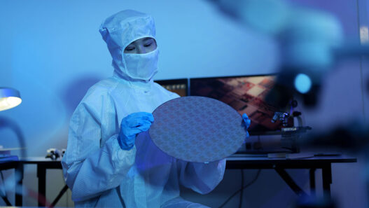
However, the products and services offered by binder do not just end with the printing of the desired functional layers. The customer can make full use of all the experience and skills of the binder Group. The newly created binder electronic solutions group provides custom-made solutions for connectors, contacts, circuit layout and automatic placement. From design and prototype to series production, the customer gets the best result from a single source. The picture shows a Printed sensor on a textured 3-D surface.
Picture shows Pad printing for printed electronics components