


Researchers from the University of Warwick and the National Research Council of Canada have engineered a strained germanium layer on silicon that allows charge to move faster than in any comparable material.
Germanium (Ge) first appeared in some of the early transistors in the 1950s and it is now drawing renewed interest as researchers take advantage of its superior electrical characteristics.
The researchers have reported the highest “hole mobility” ever measured in a material that works within today’s silicon-based semiconductor manufacturing. This could pave the way for chips that run cooler, faster, and with lower energy consumption. It’s also promising for silicon-based quantum devices.
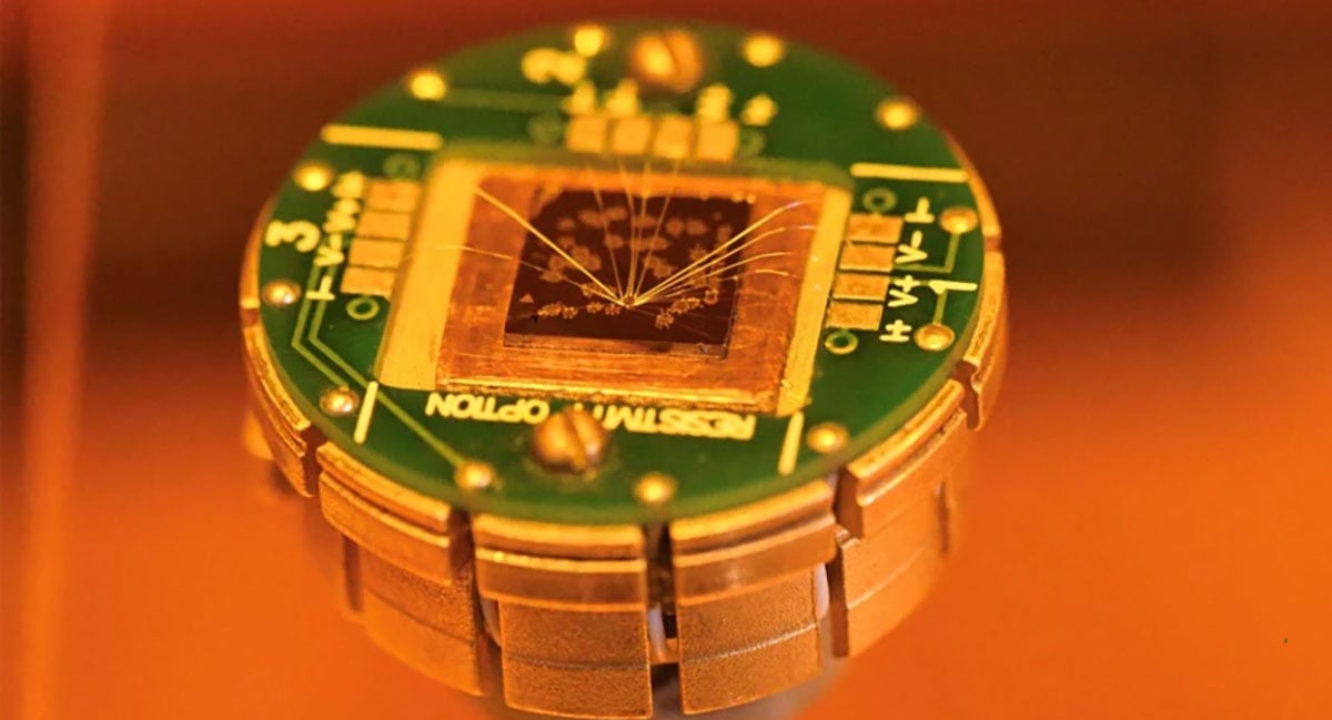
The team, led by Dr. Maksym Myronov, Associate Professor and leader of the Semiconductors Research Group, Department of Physics, University of Warwick, created a nanometre-thin germanium epilayer on silicon that is placed under compressive strain.

“Traditional high-mobility semiconductors such as gallium arsenide (GaAs) are very expensive and impossible to integrate with mainstream silicon manufacturing. Our new compressively strained germanium-on-silicon (cs-GoS) quantum material combines world-leading mobility with industrial scalability – a key step toward practical quantum and classical large-scale integrated circuits,” he explained.
By growing a thin germanium layer on a silicon wafer and then applying precise amounts of strain, the team created an exceptionally pure and orderly crystal structure that allows electrical charge to pass with minimal resistance.
When tested, the material reached a hole mobility of 7.15 million cm2 per volt-second (compared to ~450 cm2 in industrial silicon).
Dr. Sergei Studenikin, Principal Research Officer at the National Research Council of Canada, states: “This sets a new benchmark for charge transport in group-IV semiconductors – the materials at the heart of the global electronics industry. It opens the door to faster, more energy-efficient electronics and quantum devices that are fully compatible with existing silicon technology.”
These results could establish a new route towards ultra-fast, low-power semiconductor components. Applications could span from quantum information systems, spin qubits, cryogenic controllers for quantum processors, AI accelerators, and energy-efficient servers designed to reduce cooling demands in data centres.