


To meet the rising demand and requirements for flexible 2D microelectronics devices manufactured using Roll to Roll technology, we use innovative manufacturing techniques including vacuum coatings in combination with laser technology.
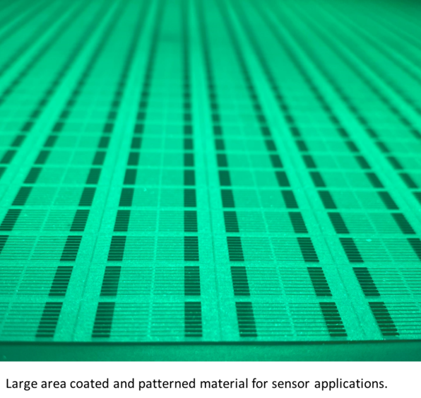
Laser patterning of sputtered coatings provides the ability to achieve high-volume production with precision, functionality, and efficiency for a wide range of flexible applications. Sputter deposition is a widely used technique for depositing thin films onto substrates. For flexible 2D microelectronics, sputtered coatings serve as the foundation for building functional devices. Sputtering involves bombarding a target material with ions to eject atoms or molecules, which then deposit onto a substrate to form a thin film. This process allows for precise control over the thickness and composition of the deposited film, making it a preferred method for creating uniform and reproducible coatings. Sputtered layers were deposited using Intellivation’s R2R Lab system. Sputtering provides an excellent method for depositing coatings uniformly over large areas, while laser patterning can create discrete devices, circuits, and other types of discontinuous features required for manufacturing. Using these two techniques in combination provides unique capabilities, particular during product development.
Photolithography requires multiple steps and is time consuming, it also requires geometric commitment of features at early stage of design. Laser patterning offers a direct and efficient way to create and define patterns on sputtered coatings including changes in geometry while providing consistent feature size and edge quality. Laser patterning uses a laser beam to selectively remove or modify specific areas of deposited films enabling the generation of intricate patterns with submicron-level precision. Control and precision of the laser is critical and the non-contact nature of laser patterning reduces the risk of contamination and damage to the underlying substrate, ideal for delicate 2D materials.
This technique provides the ability to develop and then validate a design and process in small volumes and then easily transfer to large area roll-to-roll production without changes to the laser processing equipment.
Deposition of the conductive material onto the substrate was done with Intellivation’s R2R thin film vacuum deposition Lab coater, it is then laser patterned or the laser is used to isolate regions to crystallise them for interfacing with subsequent layers. Once the substrate, layer stacks and laser variables are optimised, the next phase is to scale these devices to large area R2R processing.

The combination of laser patterning and sputtered coatings has unlocked new possibilities in the high-volume production of flexible 2D microelectronics. This innovative approach addresses the demand for devices with enhanced performance, precision, and scalability. A roll-to-roll approach offers several significant advantages in terms of efficiency, cost, and adaptability.