


Understanding these steps and the associated requirements is essential for any product manufacturer, designer, and assembly service provider. In this article, Technotronix will outline the entire process of electronic product development and guide you through the planning to the production phase in detail.
There are seven stages in the process of electronic product development:
- Market Research
- Product specification and planning
- Electronic circuit design
- Schematic Design
- BoM Generation
- Layout Design
- Associated Software development
- Mechanical chassis design
- Prototype – Testing and Debug
- Certification – Regulatory compliance
- Pre-production preparation
- Mass Production and shipment
Market Research: To start with the process, evaluate the market trends and research the product requirements in detail. It is highly recommended to do a thorough analysis at the beginning of the product development stage. There are certain points to consider while doing market research.
- Analyse the problem’s level of complexity that is intended to be addressed by your product
- Ensure a long-term demand for your product in the market
- Evaluate the competition for similar products
- Estimate a top-level costing and profit margins
Product specification and planning: With a clear understanding of the product demand and market requirements, it is suggested to plan and define the product specifications. Any product development process should start with a detailed planning of the product features, resources required, and the costing estimate. The specification document should include all the product requirements along with a concept design of functional features. Parallelly, resource and cost estimation is also done in the planning stage of the development process. This includes allocating staff and choosing service partners for component procurement, PCB fabrication, and assembly.
Electronic Circuit Design: After documentation of the product specifications, the circuit design begins. Initially, the main features of the product have to be implemented and a proof-of-concept has to be obtained. A primary Bill of materials (BoM) is generated at this stage. Some designers start with prototype design and others may prefer using development kits to evaluate their ideas. The product architect prepares a top-level block diagram outlining the product functionality. Also, a hardware architecture document and design document are drafted. A design engineer understands the product requirements by using these documents and starts with the schematic capture of the circuit, using electronic design automation (EDA) tools. The circuit design is reviewed for functionality verification and DFT (Design for testability). A BoM is rolled out to the procurement team for sourcing the components.
The netlist generated by the schematic capture will be the input for the layout design of the printed circuit board. The PCB substrate material and stack-up are decided in this stage. The layout design with component placement and routing is completed as per the DFM (Design for manufacturability) guidelines. The layout is reviewed to meet the required PCB standards (as set by the authorities like IPC – Institute for Interconnecting and Packaging Electronic circuits). The Gerber output from the software tool is handed over to the PCB fabrication provider to manufacture the PCB prototypes. The final BoM is released at this stage for the complete procurement of components and PCB assembling.
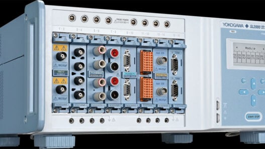
The PCB assembly and testing are usually outsourced to a contract manufacturer (CM). Choosing the right CM is very critical in the electronic product development process. The overall industry experience and the standard compliance followed by the CM are significant indicators of their process quality. Many CMs offer additional services like testing and debug support along with PCB fabrication. It is recommended to use such services from your CMs. They would be well-equipped with the necessary setups and staff support.
Prototype-Testing and Debug: Prototypes are tested for hardware functionalities. The electronic devices include microcontrollers, processors, and many programmable devices in the circuit. Associated software for these programmable devices is developed and tested on the hardware, ensuring the smooth functioning of the circuit. The product is integrated with the mechanical enclosures, followed by final testing and validation.
The electronic product goes through a series of tests and assessments for various parameters. Any required changes are noted and modified in the PCB accordingly. Only after successful completion of all the tests and procedures, the electronic product is submitted for regulatory certifications.
Certifications: Regulatory compliance: Before selling your electronic product in the market, it is necessary to obtain a few certifications based on the geographical location. Defining the class of the product and conducting the preliminary certification test are mandatory during electronic product development.
FCC (Federal communications commission) is the certification required to sell your electronic products in the US. The objective is to ensure that the electronic product’s electromagnetic radiation doesn’t interfere with wireless communication.
UL (Underwriters Laboratories) or CSA (Canadian Standards Association) is the certification for the electronic products that are plugged into an AC socket. This is required in US and Canada.
RoHS (Restriction of Hazardous Substance) certification indicates that your product is lead-free. This is required for the products sold in European Union (EU).
The electronic product’s compliance process looks quite intricate and difficult. There are service providers who can be involved in the prototype phase itself. They will provide insights into the electromagnetic characteristics of the product which can ease the product certification process.
Pre-production preparation: A completely tested and certified electronic product is cleared for bulk production. At this stage, several documents and checklists are prepared. The BoM is optimized for mass production. Storage and package standards are outlined. Logistics for the entire process is planned and any possible risks or interruption in the Bulk production is evaluated and fixed. Also, necessary setups for increased test coverages are identified and established.
Mass Production: An electronic product reaches the bulk production stage when it is completely tested and the customer is ready to purchase the product. Again, for mass production, relying on an expert contract manufacturer for PCB Manufacturing can make the whole process efficient and successful.
An experienced CM will provide alternate components if required, undertakes timely audits to maintain process quality, anticipates any possible manufacturing issues, and provides solutions. They also handle storage and shipment of the product to the customers.
Complete product development requires a well-established process and excellent teamwork. Conducting research, meticulous planning, collaborations with different teams, and following the guidelines are essential for building a successful electronic product.