


The UX8GD and UX8LD technologies combine leading-edge 40 nm CMOS process technology with NEC Electronics’ unique eDRAM process technology, and are available in memory configurations up to 256 megabits. Cell size is 0.06 square micron meters, 50 percent smaller than the company’s previous 55 nm UX7LSeD eDRAM. This translates to a 50 percent reduction in overall chip size, which contributes to lower bill-of-materials costs.
The new 40 nm technologies also leverage innovative high-dielectric (high-k) materials— such as hafnium gate dielectrics, nickel-silicide gate electrodes, and zirconium-oxide DRAM capacitors—that have been proven in NEC Electronics’ 55 nm UX7LSeD technology. These innovations lower the concentration of impurities and parasitic resistance in the channels, resulting in benefits such as lower leakage current between the drain and source, longer-term data storage, fewer variations in transistor performance, and greater performance of both logic and memory.
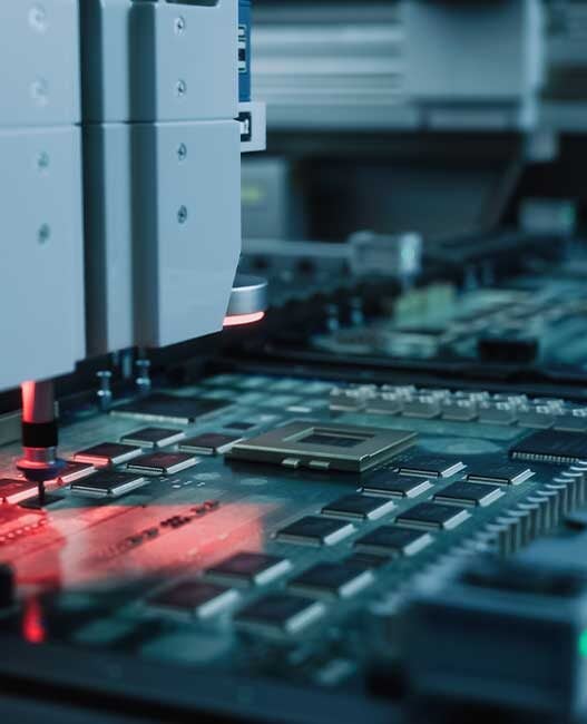
As consumers demand smaller form factors and longer operating times in mobile applications and other electronic products, semiconductor companies must deliver devices with higher performance, smaller footprints, lower power consumption, and lower costs. To meet these requirements, the development and implementation of advanced process technologies is vital.
The advantages of the new technologies featured in NEC Electronics’ 40 nm eDRAM will enable customers to more easily build electronic digital consumer products such as digital video cameras, game consoles, and mobile phones with lower power consumption and smaller and slimmer form factors.
NEC Electronics began shipment of 55 nm eDRAM samples in October 2007 and plans to ramp to volume production by the end of this fiscal year (ending March 31, 2008). Volume production of 40 nm devices is scheduled to begin by the end of the next fiscal year at NEC Electronics’ 300-millimeter wafer line at manufacturing subsidiary NEC Yamagata.