


Although we would still recognise the circuit board produced today, the process of producing it had its roots squarely in methods that had long been used in printing and artwork reproduction.
These processes have changed much since the tech breakthroughs and the manufacturing and electronic development that came to a head in the 1990s.
Here are just five of the ways that PCB manufacture was transformed from an art to a science.
The multilayer breakthrough thanks to via
It was in the 1990s that the use of multilayer surface boards became more frequent, allowing for greater complexity and speed.
The inevitable reduction in size of PCBs allowed them to be incorporated into a wider range of designs and devices.
What the introduction of blind via and buried via permitted was connection on different layers through copper-plated holes functioning as an electrical tunnel through the insulating substrate. In the past connection through layers had been allowed using plated thru-barrels, but these created an obstacle to connections to every other layer.
The result, following the introduction of via technology in 1995, was the production of High-Density Interconnect (HDI) PCBs.
These could accommodate a much denser design on the PCB and allowed the use of significantly smaller components. With multilayer HDI PCBs reliability is enhanced in all conditions, which is why the most common applications for HDI technology are computer, mobile phone components, medical equipment and military communication devices.
Via have continued to evolve, with the recent emergence of micro-via, a specific type of small via which is used on particularly high-layer-count, densely populated PCBs, which are typically performing some form of high-speed number crunching.
Leadless components and the shrinking PCB
As we’ve seen PCBs really started to shrink in the 1990s (and they haven’t stopped since). Alongside the use of micro-vias we also saw the advent of leadless component designs, such as BGAs, uBGAs, chip-scale packages and so on.
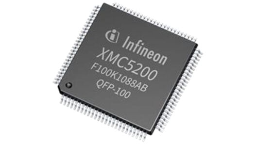
These paved the way for integrated circuits with more gates which ushered in the start of successfully embedding memories and Systems on Chip (SoC) together.
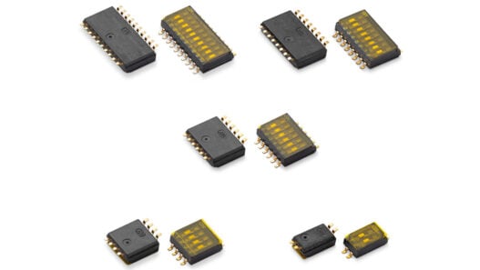
Leadless packages save space by keeping the contact points in a matrix underneath the component instead of squeezed side-by-side around their perimeter. This extra space is crucial for applications like mobile devices, tablets and wearables, where every millimetre counts.
However, leadless packages also have a great deal of mechanical strength, so they don’t separate from PCBs as easily. This is thanks to their high contact area to package ratio which allows them to withstand a great deal of pulling and shear forces.
Since leadless devices are suspended on a matrix of underside solder spheres rather that soldered pins around the perimeter, manufacturing and inspection techniques need to be much more sophisticated, but the space-efficiency and reliability benefits are compelling.
Flexible circuits transform PCB designs
It was, again, in the 1990s that flexible circuits really made their presence felt, although their history can be traced all the way back to the birth of the PCB itself.
With the first PCB manufactured by Paul Eisler less than a decade old, we find a published exploration by Cledo Brunetti and Roger W. Curtis in 1947 of creating circuits on flexible insulating materials. Indeed, by the 1950s Victor Dahlgren and Royden Sanders had already made significant advances in actually developing processes that could print and etch flat conductors on flexible base materials.
Today, flexible circuits are produced by mounting electronic devices on flexible plastic substrates (such as polyimide, PEEK or transparent conductive polyester film) or by screen printing silver circuits on polyester.
They offer several advantages for many applications. These include their potential to replace multiple rigid boards, their suitability for dynamic and high-flex applications and their ability to be stacked in various configurations.
You will find them in:
- Tightly assembled electronic packages, where electrical connections are required in three axes, such as cameras.
- Electrical connections where the assembly is required to flex, such as folding mobile phones and laptop screen hinges.
- Connections between sub-assemblies to replace the bulky and heavy wire harness, such as in cars, laptops, rockets and satellites.
- Electrical connections where board thickness, weight or space constraints are important factors.
The finishes that created new beginnings for the PCB
The range of finishes that have been introduced into PCB manufacture over the last 20 years has also greatly enhanced their suitability for use in a number of applications.
The finish is applied to ensure solderability and to create the base of electronic connection between board and device. But, the correct surface finish selection can also affect PCB reliability – and the introduction of new finishes has greatly enhanced their reliability under a number of different conditions.
- HASL
The traditional finish is Hot Air Solder Levelling (HASL) but this is now increasingly being replaced by lead-free HASL.
All HASL finishes prevent oxidation from the underlying copper but the process causes stress on the PCB and this can diminish its long-term reliability. The process is also not suitable for HDI PCBs.
- ENIG
ENIG (Electroless Nickel Immersion Gold) offers a great alternative – but one that comes with a price tag.
Ideal for fine pitch, flat surfaces, ENIG perfectly suits the modern-day HDI PCB. It can, however, carry undesirable magnetic properties and is prone to a build-up of phosphorous that may cause faulty connections and fractured surfaces.
- OSP
OSP (Organic Solderability Preservative) is a finish that can be considered for fine pitches, BGA and small components. In addition, it is less expensive than ENIG and highly repairable, but it is difficult to test and has a limited shelf life of six months.
The rise of the exotic substrate
PCB manufacture has over the years gradually settled on the glass epoxy laminate of FR-4 as its preferred material.
There is good reason for this – in terms of performance and affordability – but we have, in recent times, seen the introduction of a number of alternatives. These ceramic and metallic substrates are often suited to specialist applications, such as those requiring performance in conditions of high temperature and high power.
They include:
- Aluminium Used for parts requiring significant cooling, such as power switches and LEDs.
- Kapton A polyimide foil used for flexible printed circuits that is resistant to high temperatures.
- FR-5 Woven fiberglass and epoxy offering high strength at higher temperatures.
- G-10 Woven glass and epoxy offering high insulation resistance, low moisture absorption and very high bond strength.
- G-11 Woven glass and epoxy offering high resistance to solvents as well as high flexural strength retention at high temperatures.
- RF-35 Fiberglass-reinforced ceramics-filled PTFE (Teflon) offering good mechanical and high-frequency properties.
- Polyimide A high-temperature polymer offering excellent performance that can be used from cryogenic temperatures to over 260 °C.
The return of the art of the PCB
The diversity of today’s PCB technology requires an artist to create the perfect board for each device, application and customer.
Chemigraphic has the broad expertise and capability in each specialist area to understand and decide which technology and processes will create the right PCB for your requirements and budget.