


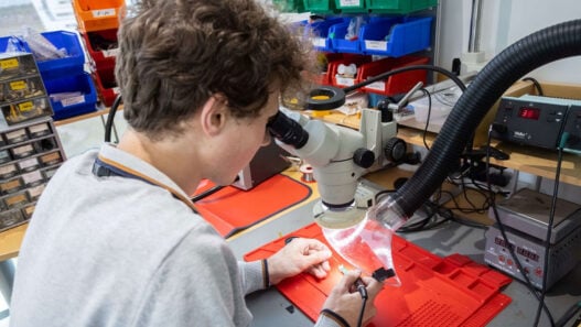
By using an electroless gold plating process with silver nanoparticles as a catalyst for an organic semiconductor, this technology enables the formation in the atmosphere of top contact-type OFET contact electrodes without the use of a vacuum environment, which requires large-scale equipment. As opposed to metallic ink, which has the same atmospheric contact formation, this technology realises the formation of a high-performance OFET as there is little damage to the organic semiconductor, and the performance of the high-mobility organic semiconductor is not affected.
Also, due to the emergence of high-performance n-type semiconductor materials in recent years, more advanced organic electronic devices can now be formed at low cost, thanks to the simultaneous formation of contact electrodes for p-type and n-type OFET mixed circuits, for which development is speeding up. For p-type organic semiconductors, the contact resistance of the contact electrodes using this technology is 0.1kΩ/cm or less, which is the lowest value currently on record in terms of the contact resistance of organic semiconductor contact electrodes formed in the atmosphere.
The atmospheric formation of a high-performance OFET with low-contact resistance electrodes and high-mobility is achieved by combining the merits of this technology with those of high-performance coating-type organic semiconductors, developed by Professor Takeya, which can be formed atmospherically. This result enables the atmospheric formation of organic electronic devices with high-speed drives, and it enables the production of high functionality electronic devices using printed electronics.
This technology is a process for the formation of contact electrodes with a gold-silver hybrid structure, which is achieved by applying a silver catalyst solution for plating that includes silver nanoparticles to an organic semiconductor crystal, after which a gold coating is applied to the substrate by immersing it in an electroless gold plating solution so that the gaps between the silver grains are filled with gold. This enables the single-process formation of low-contact resistance contact electrodes for p-type organic semiconductors, which facilitate a charge injection from gold, and n-type organic semiconductors, which facilitate a charge injection from silver.
EEJA will announce the research findings relating to this technology at the 62nd Japan Society of Applied Physics Spring Meeting, to be held 11th to 14th March at Tokai University, Shonan Campus (Hiratsuka-shi, Kanagawa).
OFET is a transistor that uses an organic semiconductor, which means that – among other characteristics unique to organic materials – it can be formed at low-temperatures, is lightweight and is flexible.
The high-performance of organic semiconductor materials has progressed rapidly in recent years, and materials are being developed with double-digit increases over the figure that was thought to be the limit for the mobility of organic semiconductors. The pioneering findings of Professor Takeya’s research group make possible the atmospheric formation of high-mobility organic semiconductors, which is expected to increase the fields of use for organic semiconductors.
While there are several methods for the formation of OFET contact electrodes, they all suffer from issues such as requiring a vacuum environment and causing damage to organic semiconductors. For example, thin film electrodes can be formed uniformly using the vacuum deposition method, but the equipment used to create a vacuum environment is incredibly expensive, and the loss of materials is huge. Also, while electrode formation in the atmosphere is possible using metallic ink and metallic paste, it also requires the inclusion of organic solvents, high-temperature sintering, and hardening by means of ultra-violet rays, which damages the organic semiconductor, and does not achieve sufficient results as a transistor.
This is why, in September 2014, EEJA, together with Professor Takeya’s research group, jointly developed plating-process contact electrode formation technology for p-type organic semiconductors. In order to stably form electrodes for organic semiconductor crystals, EEJA developed gold nanoparticles as an electroless plating catalyst. The contact resistance of the contact electrodes formed using this technology is 0.7kΩ/cm, which is a remarkably low contact resistance for atmospheric formation contact electrodes.
Also, Professor Takeya’s research group developed a coating-type organic semiconductor that could be formed in a short time in the atmosphere with a large-surface thin film with uniform crystal orientation, and a mobility (which is the deciding factor in the performance of semiconductors) that greatly surpasses that of conventional organic semiconductors at 10cm2/Vs or more.
Because OFET has the characteristics of being printable, lightweight and flexible, EEJA anticipates such device developments as flexible displays and disposable RFID tags. Currently, development is mainly progressing for devices that use p-type organic semiconductors, but the development of all-flexible displays and wearable computers, which require advanced circuitry and bendable driver ICs, also requires p-type and n-type OFET mixed circuitry and both OFETs must operate at high speeds. This jointly developed technology contributes to technical innovation in connection to organic electronic devices. EEJA will continue to find further solutions for utilisation in organic electronic devices.