


The good news is that antenna manufacture is undergoing a revolution. Whilst print-based graphene or CNT-based thin-film antennas are yet to come on stream, many materials science-based techniques are already informing the way antennas are constructed, helping end designers to breach the trade-off between the limits imposed by the laws of physics and the size, weight, power consumption and performance attributes that are commonly required.
Whilst the relationship governing small antenna design remains the link between size, gain and bandwidth, it has become easier to optimise a design for any of these parameters, though the trade-offs are such that all three can’t be optimised in the same design. For example, if we widen the bandwidth (lower the quality factor, Q), the antenna would have to be bigger. If we reduce the gain (reduce the efficiency), we can increase the bandwidth. Manufacturers have tried to bend the rules by integrating multiple antennas into a single package to save space, but often at the expense of efficiency and power consumption. Tuneable antennas are another idea – if only one part of the band needs to be covered at any one time, a smaller, narrower band antenna can be made that is dynamically tuned to the required frequency. Again though, power consumption may suffer.
Changing substrates and shape
An antenna’s substrate material has a huge effect on its performance. If permittivity and permeability of the material can be increased (perhaps by using new specially-designed robust ceramics) more bandwidth can be achieved in a smaller volume. And if the permittivity of the material can be varied throughout its volume, it can also be used to ‘focus’ waves, another way to cheat the physical constraints and make thinner components.
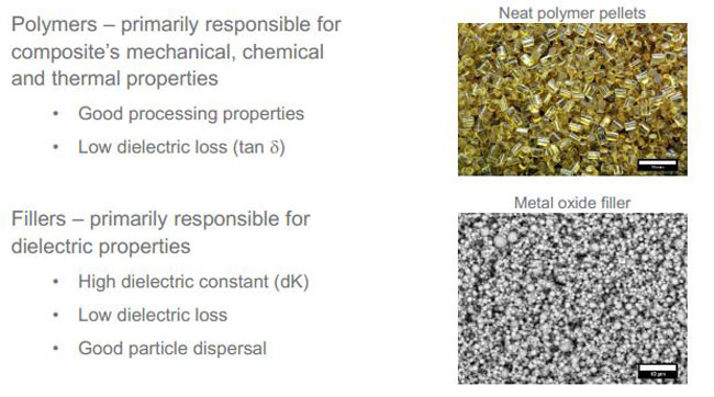
TE Connectivity’s custom composite materials are typically a combination of a polymer material, chosen for its processing properties (mechanical, chemical and thermal), mixed with a metal oxide filler material, which is responsible for the dielectric properties of the composite. These filler materials are specially engineered to have as high a permittivity as possible. To create custom antennas, the right materials and their relative proportions are selected to yield the desired performance. The two materials can then be physically mixed to create the substrate, either by stirring filler particles into melted polymer, or by laminating the materials in alternating layers, or by 3D printing to produce exotic shapes.
Indeed, antenna manufacturers have long experimented with different shapes. Helical (or coiled) elements have been a popular variant of monopoleantenna (astraight rod-shaped conductor, mounted perpendicular to the ground plane), though they are somewhat anodyne in name when one considers other types that include the whip, rubber ducky or umbrella! Notably, dipole antennas (two straight rods or wires oriented end-to-end on the same axis) feature similarly interesting forms such as the foldeddipole, shortdipole, bow-tie or batwing!Metallisation
As well as the substrate, the metallisation of antennas also has a significant effect on performance. Three broad techniques are commonly used.
Formed metal antennas are made by stamping and bending sheet metal, resulting in high conductivity and high throughput devices. However, this method can’t create the 3D shapes needed for today’s more complex designs. It can also be expensive to revise designs, as new tooling is required each time.
MID (moulded interconnect device) antennas rely on plating metal onto a carrier to form a conductive surface, and there are many different ways of doing it. The substrate can simply be moulded, with a catalyst that allows plating onto that area applied via two-shot moulding. Moulding creates high conductivity antennas, though expensive tooling is required to create the moulds.
An alternative to moulding is Laser Direct Structuring (LDS), which uses a substrate that contains the plating catalyst. The catalyst in the plastic is activated via laser, in the specific areas where metallisation is required, so the metal antenna shape is formed during plating. This method is an entirely digital process, using the output from CAD programs, so there’s no tooling expense, but adding the catalyst to the resin has a cost penalty.
Printing conductive ‘inks’ in pre-defined patterns is another metallisation technique, which can be used with a wide variety of substrate materials. The inks are silver, tin or copper particles mixed with an organic binder and solvent, so conductivity is generally lower than for formed or plated metal. However, the ink formulation and thickness can be tailored to conductivity, adhesion, and environmental stability requirements.
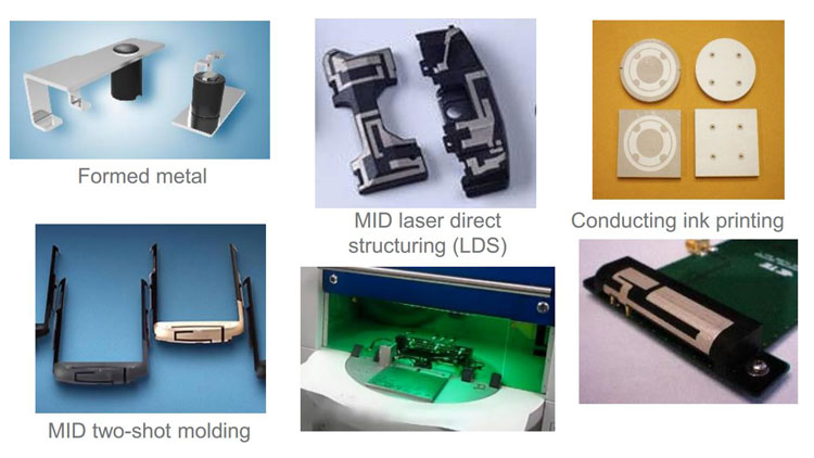
The easiest printing method is screen-printing, which requires some tooling but this is at very low cost. Feature sizes as small as 50µm can be achieved this way, with a thickness of 10-30µm. Pad printing, essentially rubber stamping, can produce thinner layers, while computer-controlled inkjet printing can be used on 2D or 3D shapes at the expense of thickness.
The right combination of materials and techniques can produce antennas that push the boundaries of size, gain and bandwidth for the next generation of connected electronic products. TE Connectivity has many years’ experience designing and optimising substrate materials and manufacturing techniques to produce custom antennas.
Click here for more information.