


Written by Paul Yeh, Applications Engineer, Renesas Electronics.
Serial Peripheral Interface (SPI) is a widely used high-speed communication protocol—typically operating above 1MHz—that enables seamless data exchange between a microcontroller (MCU) and multiple peripheral devices. By leveraging key signals such as Chip Select (CS), Serial Clock (SCLK), Master-Out-Slave-In (MOSI), and optionally Master-In-Slave-Out (MISO), this design demonstrates how SPI can be optimised for multi-device synchronisation and streamlined data transfer. Whether you’re designing compact embedded systems or expanding control across multiple components, this setup offers a practical and high-performance solution.
There are two ways to connect multiple devices:
- In Figure 1, an MCU provides multiple Chip-Select (CS) signals to corresponding peripheral ADC devices. Each Chip-Select signal is independently connected to a peripheral device. This method of SPI connection requires complicated PCB layout/subnodes and additional GPIO utilisation. In addition, the MCU cannot capture ADC data from the ADC devices synchronously.
- Daisy-Chain SPI, as shown in Figure 2, is developed to simplify subnodes using only one Chip-Select (CS) signal. The MCU provides a single Chip-Select (CS) signal that is sent to all peripheral ADC devices. Meanwhile, MOSI and MISO signals are integrated using a daisy-chain configuration. While the CS signal activates all peripheral ADC devices, each ADC device can transfer its own data in sequence to the MCU. Therefore, the MCU can capture multiple instances of ADC data simultaneously.
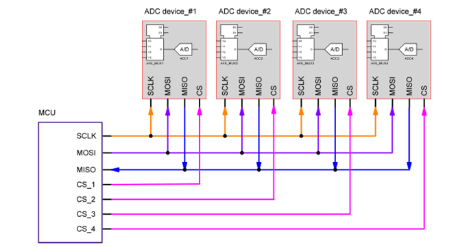
Figure 1. General SPI Connection Diagram

Figure 2. Daisy-Chain SPI Connection Diagram
The SLG47011 is comprised of a diverse collection of digital and analog marcocells for AFE applications. One 14-bit SAR ADC and one 4-channel PGA (shown in the Block Diagram of the SLG47011 in Figure 3 are used to perform Analog Front-End signal capturing. The PGA is capable of operating in different configurations including single-ended mode and differential mode. Additionally, the reference voltages used by the PGA and ADC can be configured independently as needed. The ADC supports resolutions ranging from 8 bits to 14 bits. Moreover, the SLG47011 offers four Buffer blocks in which averaging and over-sampling functions are used to process ADC data.
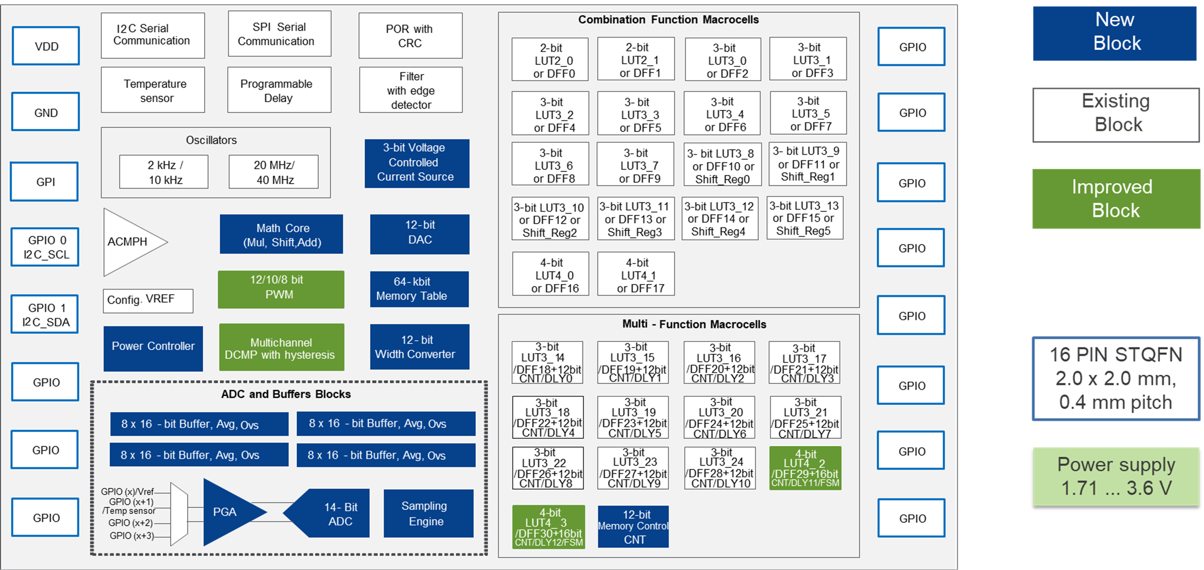
Figure 3. SLG47011 Block Diagram
Design principle
Figure 4 shows the system diagram of a Daisy chain SPI connection. Each SLG47011 provides 3 external AFE inputs (Pin7, Pin8, and Pin9). The SPI interface I/O inherited from the SLG47011 provides the CS(PIN3), SCLK (PIN5), MOSI (PIN4) and MISO (PIN6) connections. To create Daisy-chain SPI based on inherited SPI, we use the internal digital blocks of the SLG47011 and utilise GPIO Pins to synthesise the required function. Pin16, Pin15, and Pin10 are assigned to connect the inherited SPI interface I/O directly. Compared to an Inherited SPI interface I/O, the Daisy Chain SPI interface I/O represented by CS (Pin13), SCLK (PIN5), MOSI (PIN12), and MISO (PIN11). Therefore, MCU would read the data via Daisy Chain SPI interface I/O. Figure 5 shows the Pin connections of a single chip as a reference. Since the inherited SPI macrocell in the SLG47011V cannot support an internal connection using Matirix I/O, GPIO Pins are used to carry out the design. Since the propagation delay of the GPIO Pins is greater than that of the Matrix I/O, it is estimated that the SPI baud rate frequency (SCLK) should be limited to less than 3.4MHz.
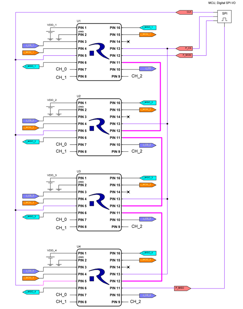
Figure 4. System Diagram of using Quad-Chips in a Daisy-Chain SPI Connection
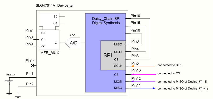
Figure 5. Pin Assignment for a Single-Chip Implemented in a Daisy-Chain SPI Design
A diagram of the SPI signal sequence of Daisy chain SPI is shown in Figure 6. The master MCU device sends one SPI command to collect required data from all peripheral devices (chip_1~4). Once an individual peripheral device receives a command, it will transfer internal data via the inherited SPI macrocell. To manipulate the internal data in sequence, the digital synthesis subcircuit, in Figure 5, needs to initiate the serial-in/serial-out process. Since the CMD signal or Data signals will be propagated through a string of peripheral devices, Pin 10 and Pin 15 are regarded as the main subnodes and must succeed in transferring data and receive the CMD signal, separately. SCLK can be used to allocate the Data sequence transfer and interconnection period.

Figure 6. SPI Signal Sequence Diagram of Daisy Chain SPI
In Figure 7, the block diagram illustrates the basic digital synthesis design. SW_A and SW_B are the switches used for sending CMD and Data. The CNT/DLYs + LUTs block provides the CS signal to the inherited SPI block. The Inherited SPI block transfers the corresponding data associated with the unique CMD in all chips. The SHR shifts the data from the inherited SPI block using its specific register lengths setting. Therefore, data from each individual chip is arranged in order. We utilise the macrocells of the SLG47011V to fulfil this required functionality.
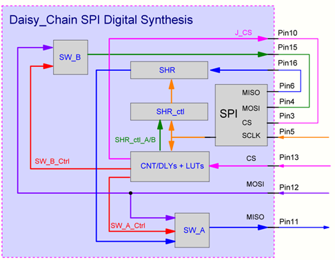
Figure 7. Block Diagram of the Daisy Chain SPI Digital Synthesis
GreenPAK design internal block configuration
All GreenPAK Designs shown in the Go Configure Software are presented in Figure 8 ~ Figure 11. The configuration descriptions follow.
.png)
Figure 8. GreenPAK Designer Schematic (Daisychain_SPI_CHIP_1.aap)
.png)
Figure 9. GreenPAK Designer Schematic (Daisychain_SPI_CHIP_2.aap)
.png)
Figure 10. GreenPAK Designer Schematic (Daisychain_SPI_CHIP_3.aap)
.png)
Figure 11. GreenPAK Designer Schematic (Daisychain_SPI_CHIP_4.aap)
As shown in Figure 7, SW_A and SW_B functions are accomplished by using LUT macrocells. The logic configuration of these macrocells is shown in Figure 12.
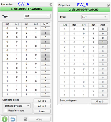
Figure 12. LUT Configuration for SW_A and SW_B.
Also shown in Figure 7, the SHR (Shifter register) processes the data from the inherited SPI block. To ensure the data sequence is integrated into the final MOSI bus of chip_4, we must use three SHR macrocells to output data in sequence. In our design, chip_1 is not equipped with a SHR block due to data first-in-first-out principles, as shown in Figure 8. The total register length settings of the SHR blocks are set to 18. This configuration is shown in Figure 13.
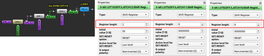
Figure 13. Configuration for the SHR Block
Referring back to Figure 7 and the schematics in the GP file, this design uses multiple combination blocks for five control signals: SW_A_Ctrl, SW_B_Ctrl, J_CS, SHR_ctl_A, and SHR_ctl_B
The first combination block (SW_A_Ctrl) consists of CNT6 and LUT21. Output is assigned to control SW_A.
- For Chip 1: CNT6 Counter data = 22.
- For Chip 2: CNT6 Counter data = 38.
- For Chip 3: CNT6 Counter data = 54.
- For Chip 4: CNT6 Counter data = 70.
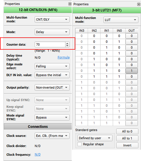
Figure 14. Configuration for the first Combination Block
The second combination block (SW_B_Ctrl) consists of CNT4 and LUT4. Output is assigned to control SW_B. All macrocells are given the same configuration. For chip_1~4: CNT4 Counter data = 22.
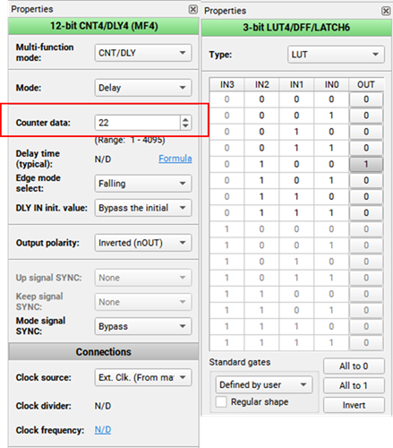
Figure 15. Configuration for second Combination Block
The third combination block (J_CS) consists of CNT3, CNT4, LUT1, and LUT17. Output is assigned to generate a variant CS signal forward to Pin10. All macrocells are given the same configuration. For chip_ 1~4: CNT2 Counter data = 38.
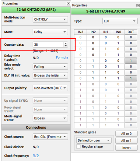
Figure 16. Configuration for the third Combination Block
The fourth and fifth combination blocks (SHR_ctl_A and SHR_ctl_B) are used to arrange the data transfer sequences. For chip_1~4: CNT5 and CNT8 Counter data = 14.
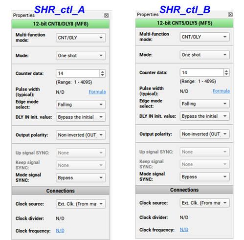
Figure 17. Configuration for the fourth and fifth Combination Blocks
As shown in Figure 6, the MISO bus of Chip 4 transmits data forward to the MCU. In Figure 18 it is shown that SHR_reset is used to blank the CMD transfer in SW_A of Chip 4.
![]()
Figure 18. CMD Blank Block
For inspecting the sequence of data transfer in Daisy Chain SPI, we assign the FSM1 macrocell to store a specific counter data. The design and configuration are shown in Figure 19.
- For Chip 1: Counter data = 8,601 (h21, h99) For Chip 2: Counter data = 16,331 (h3F, hCB)
- For Chip 3: Counter data = 9,173 (h23, hD5) For Chip 4: Counter data = 12,291 (h30, h03)
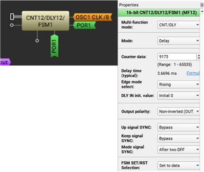
Figure 19. Configuration for Specific Data Inspection
The prototypical Daisy chain SPI is eventually completed. Next, we add the ADC block for multiple AFE applications. As shown in Figure 20, we create four AFE channels associated with the ADC block. Three external AFE channels are assigned to Pin 7, Pin 8, and Pin 9, respectively. The PGA macrocell is configured in single-ended mode for the AFE channels. Additionally, the internal AFE channel is used to monitor the temperature sensor.

Figure 20. Three External AFE Channels associated with ADC
Figure 21 shows the configuration for the reference design.
The ADC macrocell is configured with 14-bit resolution and channel sampling period of 400μs. ADC data is configured in Buffer Mode to transfer data to Buffer macrocells, and the Buffer data can be read via SPI protocol directly.
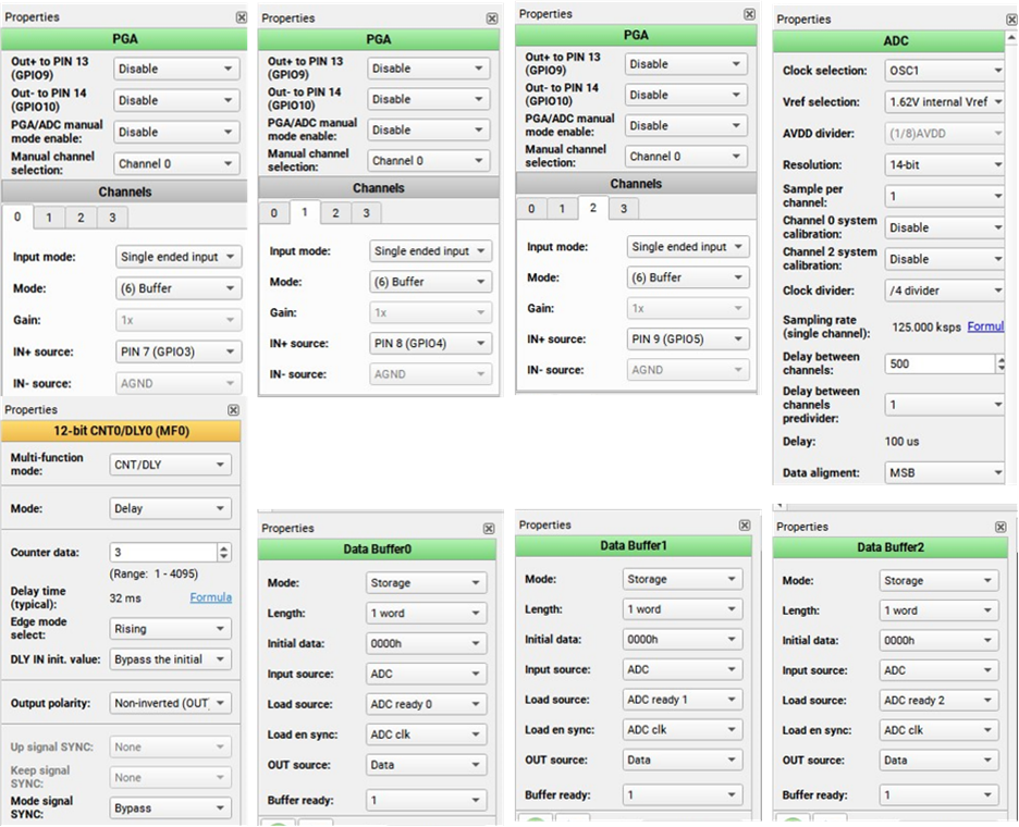
Figure 21. Configuration of Multiple AFE Channel Block
Simulation results
The simulation of Chip 2 is shown in Figure 22.
The CS signal transmitted by the MCU can be reshaped to trigger the inherited SPI to prepare Chip 2 data.
CMD is received and forwarded to MISO.
The SHR block works to propagate the Chip data in turn.
The MISO signal from Chip 2 outputs CMD and the Data of Chip 1 and the Data of Chip 2.
This single chip simulation also applies to the behaviour of the other Chips as well.
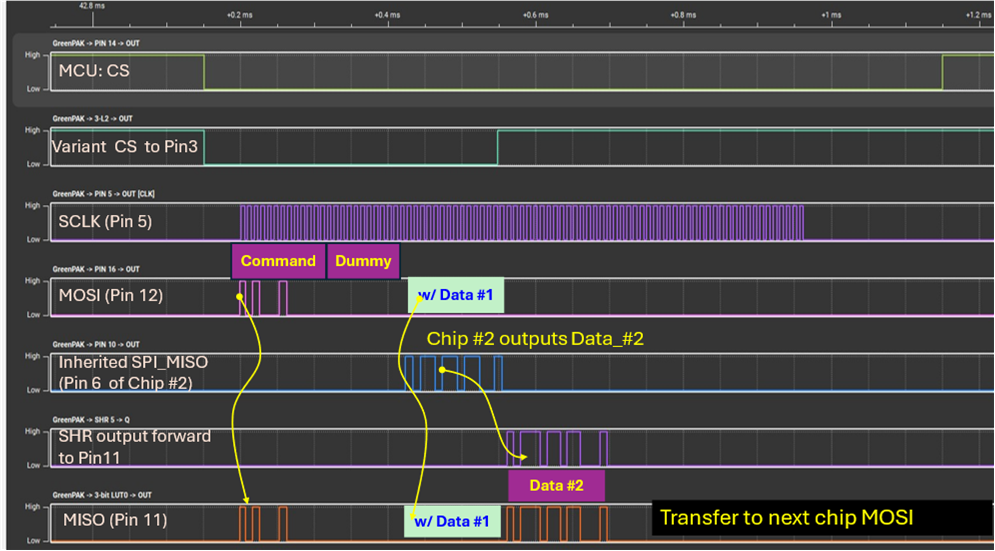
Figure 22. Simulation Results
Design verification using hardware prototype
After programming the NVM on each chip, we can prepare four SLG47011V daughterboards and carry out the wire connection, as shown in Figure 23. A Digilent ADP3450 Portable oscilloscope is set up to provide the required SPI send/receive test-pattern and protocol analyser.
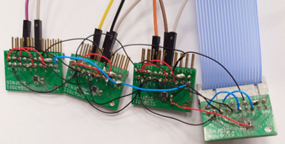
Figure 23. Hardware Prototype and Bench
Basic Testing conditions: VDD = 3.3 V to the four chips; SPI SCLK frequency = 3.4MHz (provided by the ADP3450)
Inspection: reading data from DLY/CNT, [h0139, h013A]
To inspect the SPI communication and data sequence, the quad SLG47011V prototype is equipped with specific data, independently. The specific data are regarded as check-code allocated to each individual chip’s FSM1 macrocell. From the validation results, the SPI MISO data sequence indicates the data permutations in arrangement. The protocol analyser collects all specific data by sending an SPI command [hA2, h26]. Every chip reflects its individual data including [h01, h39] (FSM1_Data_MSB) and [h01, h3A] (FSM1_Data_LSB).
- Chip 1: specific counter data in FSM1 macrocell is given h2199.
- Chip 2: specific counter data in FSM1 macrocell is given h3FCB.
- Chip 3: specific counter data in FSM1 macrocell is given h23D5.
- Chip 4: specific counter data in FSM1 macrocell is given h3003.
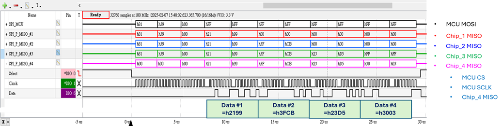
Figure 24. Sequence Inspection for Daisy Chain SPI
Capturing ADC Data: Reading Channel_0 from Buffer0, [h2202, h2203]
This validation shows that the protocol analyser collects every chip’s channel_0 data by sending an SPI command [h22, h02]. Every chip reflects its individual data including [h22, h02] (BUFFER0_Data_MSB) and [h22, h03] (BUFFER0_Data_LSB). BUFFER0_Data collects the data from ADC channel_0.
- Chip 1: Channel 0 is given 0.6 V, Buffer0 return ADC data= h17F1 for 0.6061 V
- Chip 2: Channel 0 is given 0.2 V, Buffer0 return ADC data= h07C6 for 0.1968 V
- Chip 3: Channel 0 is given 1.0 V, Buffer0 return ADC data= h27F8 for 1.0118 V
- Chip 4: Channel 0 is given 0.0 V, Buffer0 return ADC data= h0002 for 0.0002 V
Conclusion
Using four SLG47011V devices in a daisy-chained SPI configuration helps simplify PCB layout and may reduce the number of required subnodes. The system supports an SCLK baud rate of up to 3.4MHz, allowing fast and efficient data transfer. Each SPI command can trigger synchronised ADC data collection from all connected SLG47011V chips. Test results confirm that this setup accurately captures ADC readings from each individual channel. To ensure precise measurements and minimise noise, a complete and well-planned PCB layout is strongly recommended. This design highlights the SLG47011V’s value in compact, high-speed analog signal processing systems.