


Designers must balance system size and power consumption while enabling more precise signal measurements at higher bandwidths, says Mark Berarducci, engineer at Texas Instruments.
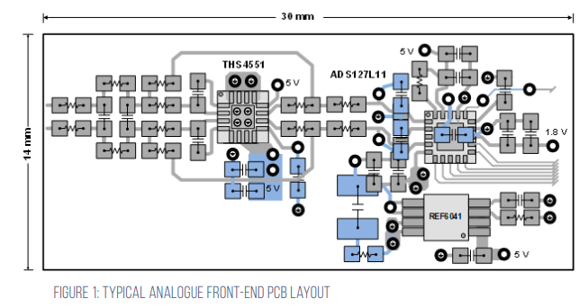
Product design is directly related to the size of the electronics within. Technological advances mean that the converter is no longer the largest component in a data acquisition system. Figure 1 shows a layout of a data acquisition system using the THS4551 fully differential amplifier with fourth-order low-pass filter, the REF6041 voltage reference with integrated buffer and the ADS127L11 wideband ADC.
ADC power consumption
Minimising power consumption extends the battery run time of portable equipment while low power consumption can translate to smaller, lighter equipment, reducing four parallel-connected battery cells to three, for example.
Reduced power consumption also benefits offline-powered equipment. Low power dissipation reduces temperature rise within the enclosure, reducing the average junction temperature of the ICs, in some cases reducing or eliminating forced air cooling. Conversely, eliminating vent slots from product enclosures or control panels reduces the amount of dust and vapours condensing on the PCB surface.
Reducing power consumption can also translate to an overall smaller size of the power-supply magnetics, for smaller enclosure options.
ADC resolution
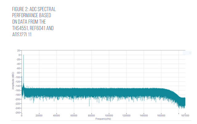
Contributing noise sources can limit measurement resolution in a data acquisition system (from the reference voltage and input signal conditioning circuit). Arguably, the primary factor of system resolution for any industrial equipment measuring AC signals, such as vibration/acoustic monitoring and general purpose data acquisition, is the converter. It should be free of tones and other spurious frequencies that limit measurement resolution, with low broadband noise to resolve small signal levels and low distortion for good spectral performance (Figure 2).
DC bandwidth
During the precision acquisition of AC signals, the converter should have frequency characteristics approaching the ideal: a flat passband with low ripple, a sharp transition band to conserve as much bandwidth as possible and a stopband in full effect at the Nyquist frequency to minimise signal aliasing. Once signal aliasing occurs, the signal cannot be corrected by post-processing, so it is important to attenuate the out-of-band signals as economically as possible.
A wideband delta sigma ADC provides these filter properties, including anti-aliasing. A wideband (or brick-wall filter) comes from the digital filter with the pass band, transition band and stopband performance. The filter is only made possible by oversampling and for the best power and resolution metrics, is usually used in conjunction with a delta sigma ADC (see Figure 3).
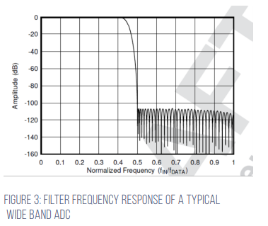
The stopband attenuation of the wideband filter eliminates the need for an external anti-alias filter – typically needed with a successive approximation register (SAR) ADC – both of which are designed to provide signal attenuation at the Nyquist frequency. An equivalent order of an external anti-alias filter would be very high and expensive to implement. Avoiding an external filter saves design and component costs, as well as in-band phase shift.
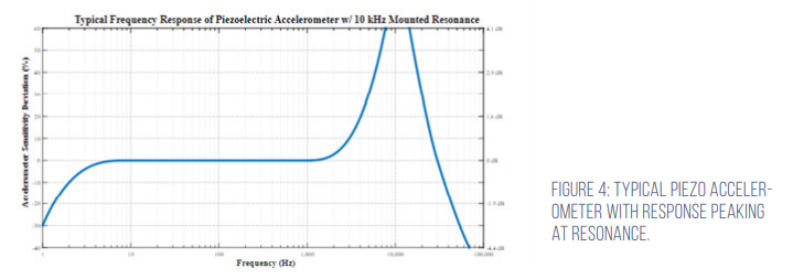
The anti-aliasing property of the converter’s wideband filter rejects the out-of-band signals generated by the piezo sensor. For example, piezo accelerometer sensors have a resonance frequency of up to +20dB above normal signal levels which occurs just before the sensor’s response rolls off. If the resonance is excited, the resonant peak (as well as other frequencies occurring above Nyquist) can alias to the passband, leading to incorrect frequency analysis of the signal. Figure 4 shows the frequency response of a piezo accelerometer with typical high-frequency resonance peaking.
One drawback of integrating a wideband filter into the converter is the silicon die area required by the logic gates. The IC designer can leverage the small transistor size with associated low threshold voltage to reduce power consumption, but at the same time will require the transistors to achieve excellent analogue section noise and linearity performance.
TI has developed an IC process that meets both criteria. A small transistor geometry reduces stray capacitance (C) associated with the logic gates, resulting in lower internal power loss. The following equation expresses the power loss (P) operating at clock frequency (f) and operating voltage (V):
P = V2 × f × C
Reducing the threshold voltage reduces the power loss associated with the V2 power supply. Reduced coupling of digital switching noise to the analogue section reduces the peak switching currents by virtue of the small transistor size used in the ADC digital section.